 ,*,?,2)
ANALYSIS OF THE PIEZOTRONIC EFFECT OF A PIEZOELETRIC SEMICONDUCTOR FIBER UNDER MUTIPLE LOCAL TEMPERATURE LOADINGS 1)
Cheng Ruoran*, Zhang Chunli,*,?,2)通讯作者: 2)张春利, 副教授, 研究方向: 多场耦合力学、智能材料与结构力学、压电电子/光电子学. E-mail:zhangcl01@zju.edu.cn
收稿日期:2020-04-20接受日期:2020-04-20网络出版日期:2020-09-18
| 基金资助: |
Received:2020-04-20Accepted:2020-04-20Online:2020-09-18
作者简介 About authors

摘要
温度改变产生的极化电势可对压电半导体结构内的物理量进行有效调控, 这在穿戴电子器件及与温度相关的半导体电子器件中有重要工程应用价值. 本文针对在多个局部均匀温度变化作用下的压电半导体杆结构, 采用一维热压电半导体多场耦合方程, 基于线性化的漂移-扩散(drift-diffusion)电流模型导出了问题的解析解. 以两个局部温度载荷情况为例, 数值分析了局部温度改变对压电半导体内位移、电势、电位移、极化强度、载流子分布等物理场的影响. 对于温度改变较大的情况, 在COMSOL软件的PDE模块中, 采用非线性电流模型, 进行数值模拟. 研究结果表明: 由于两个局部区域的温度改变, 在半导体杆内形成了局部势垒和势阱, 不同的温度改变量和作用区域会产生不同高度/深度的势垒/势阱, 为基于压电半导体的热压电电子学器件结构设计提供了理论指导.
关键词:
Abstract
The polarization potential resulted from a temperature change through a series coupling effects can significantly change physical fields in piezoelectric semiconductor (PS) structures, which has been found important engineering applications in wearable electronics and temperature-related semiconductor electron devices. Using the one-dimensional multi-field coupling model for thermo-piezoelectric semiconductors, we study the effect of multiple local temperature changes on the behaviors of PS fibers. Based on the linearized current constitutive relations, we obtain the analytical solutions. For instance, a PS fiber under two local temperature changes is numerically studied. The effect of local temperature changes on the distributions of the displacement, potential, electric displacement, polarization and carrier are examined. For large temperature changes, we conduct a nonlinear analysis by COMSOL using the nonlinear current model. The numerical results show that the potential barrier and well produced by the temperature changes through a series of coupling effects depend on the magnitude of the temperature change and the thermal load position. This provides a useful theoretical guidance in the designing of devices.
Keywords:
PDF (1724KB)元数据多维度评价相关文章导出EndNote|Ris|Bibtex收藏本文
本文引用格式
程若然, 张春利. 多个局部温度载荷下压电半导体纤维杆的压电电子学行为分析 1). 力学学报[J], 2020, 52(5): 1295-1303 DOI:10.6052/0459-1879-20-128
Cheng Ruoran, Zhang Chunli.
引言
第三代半导体是兼具压电性和半导体双重物理属性的压电半导体材料, 在未来信息、能源、国防和航空航天等领域有巨大应用前景. 事实上, 早在20世纪60年代就有****尝试利用压电半导体的声电效应实现声波器件[1]. 然而, 由于早期合成的压电半导体材料的压电效应非常微弱, 这限制了其在实际工程中的应用. 近年来, 以氧化锌(ZnO)纳米结构[2-4]等为代表的具有较大压电效应的压电半导体被成功制备, 引起了****们的广泛关注, 已被用于纳米发电机[5-7]、 声电荷输运器件[8]、 场效应晶体管[9-10]和应变/气体/湿度传感器等[2,11]功能器件上. 近年来, 关于压电半导体的研究主要集中在: 通过施加外力, 利用压电效应产生的压电势对肖特基结和PN结结区载流子的输运、产生、分离和复合等半导体特性的调节与控制上, 由此形成了压电电子学和压电光电子学[12-13]两个崭新的研究领域.开展压电半导体多场耦合力学行为方面的理论研究, 可为利用压电电子/光电子学效应提升半导体器件性能或开发新型半导体器件[14]提供重要理论指导. 在已有的理论研究中, 大多数工作仅考虑压电效应, 研究机械载荷对压电半导体内多场耦合行为的影响[15-28]. 例如, Zhang等[16-17]利用线性化方法理论研究了压电半导体纤维杆内机械载荷对压电电子学效应以及机电场的影响. 事实上, 除了压电性外, 绝大多数压电半导体材料还具有热释电性、热弹性、热电效应等与温度有关的耦合效应[29]; 因此, 温度的改变必会使其产生极化电势. 无论是考虑消除热效应(如电子器件散热、热疲劳、热应力造成结构强度问题等)对器件性能的影响, 还是主动利用温度改变产生的极化电势开发与温度相关的新型半导体器件, 理论研究温度对压电半导体结构的多场耦合力学行为的影响都是非常亟需的. 最近, Cheng等[30-31]同时考虑热弹性、热释电性和压电效应, 理论研究了均匀温度改变对一维压电半导体杆及一维压电半导体复合结构内部机电场的影响, 结果表明了利用温度改变调控压电电子学效应的可能性; 随后, Cheng等[32]通过对n型压电半导体纤维施加一个局部均匀温度载荷, 发现在其内部产生局部势垒和势阱——它们阻碍载流子的定向运动, 出现了类似PN结单向导通或开关的性质. 可以想象: 如果施加多个局部温度载荷, 则会形成多个局部势垒和势阱, 施加的局部温度载荷的大小和载荷之间的距离的选择会使内部呈现出丰富多样的多场耦合行为. 然而, 文献[32]中单个局部温度载荷的工作不适用于此种情况. 因此, 我们进一步研究具有代表性的两个局部温度载荷作用下压电半导体纤维杆的多场耦合力学行为.
1 热压电半导体纤维杆的一维方程
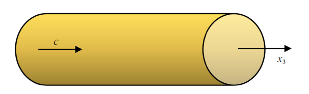
在此前的工作[30-32]中导出的热压电半导体纤维杆的一维方程仍然适用, 其详细推导过程在这里不再赘述, 仅列出与本文相关的方程. 考虑如图1所示的一根均匀掺杂的具有6 mm对称性的压电半导体细长杆, 其极化方向沿着轴向$x_{3}$.图1
 新窗口打开|下载原图ZIP|生成PPT
图1压电半导体纤维杆示意图(6 mm)
Fig.1A piezoelectric semiconductor fiber of crystals of class (6 mm)
在初始参考温度$\varTheta_0 $下, 压电半导体内部的施主和受主密度分别为$N_D^+$和$N_A^- $, 空穴和电子密度分别为$p_0 =N_D^+ $和$n_0=N_A^- $. 当结构受到一个均匀温度变化$\theta =\varTheta -\varTheta _0 $到达温度$\varTheta $时, 其内部空穴和电子密度可写为
其中, $\Delta p$和$\Delta n$是压电半导体受到均匀温度变化后, 空穴和电子密度的增量. 运动平衡方程、静电高斯方程、空穴和电子的电荷守恒方程分别为[32]
其中, $T_{33}$, $\rho$, $u_{3}$, $D_{3}$, $q$, $J_3^p $和$J_3^n$分别是轴向应力、密度、轴向位移、轴向电位移、基本电荷、轴向空穴和电子电流密度. 式(2)中的应力、电位移及空穴和电子电流密度的本构方程为
注意, 在式(4)中对于载流子密度增量很小(即$\Delta n<<n_0 $和$\Delta p<<p_0)$的情况作了线性化处理. $S_{33}$和$E_{3}$分别为轴向应变与电场强度, 它们是
式(3)中的等效材料常数为
在式(4)和式(6)中, $\mu _{33}^p $, $\mu _{33}^n $, $D_{33}^p $, $D_{33}^n$, $s_{33}^E $, $d_{33} $, $\alpha _{33} $, $\varepsilon_{33}^{\rm T} $, $p_3$分别为空穴迁移率、电子迁移率、空穴扩散系数、电子扩散系数、弹性常数、压电常数、热膨胀系数、介电常数、热释电系数. 上述的相关材料参数均在参考温度$\varTheta _0 $下定义, 且$\mu _{33}^p $, $\mu_{33}^n $, $D_{33}^p $和$D_{33}^n$满足在该参考温度下的爱因斯坦关系
其中, $k_{\rm B} $为玻尔兹曼常数, 将式(3)~式(5)代入式(2)中可得到4个关于$u_{3}$, $\varphi$, $\Delta p$, $\Delta n$的二阶常微分方程. 根据式(4)中是否使用线性化, 这4个常微分方程可以是线性的或非线性的.
2 多个局部温度作用下的压电半导体杆内的多场耦合行为
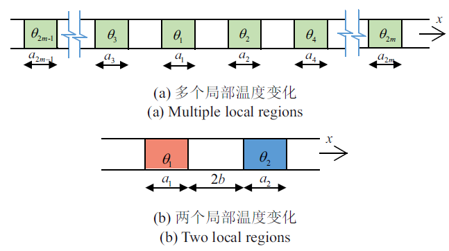
考虑如图2所示的一根n型掺杂的无限长氧化锌压电半导体杆, 在无限远端为电学开路条件, 白色区域表示该区域温度为参考温度$\varTheta _0 $, 绿色区域表示该区域发生了相对温度改变. 当杆在如图2(a)所示的2$m$个不相邻区域(长度范围为$a_{i}$, $i=1,2,\cdots, 2m)$, 有局部的均匀温度改变$\theta _i $, 杆内会产生轴向变形. 为得到问题的解析解, 用方程(4)中线性化的电流模型(注意:线性化方法只适用于小的温度改变情况). 在2$m$个局部温度载荷作用下, 结构可分为4$m$+1个求解区域, 数学上很容易由式(2)中的控制方程和式(3)与式(4)的线性本构方程求出问题的解. 对应第$i$个区域内的电子密度增量$\Delta n_i $, 电势$\varphi _i $和位移$u_{3i}$有如下形式的通解图2
 新窗口打开|下载原图ZIP|生成PPT
图2压电半导体杆受局部温度载荷作用示意图
Fig.2A piezoelectric semiconductor fiber under local temperature changes
其中, $C_{i1}$, $C_{i2}$, $\cdots$, $C_{i6}$为待定系数. 由边界条件、界面连续条件以及选取零电势点和为消除刚体位移而选取零位移点即可确定所有待定系数, 这样就得到了多个局部温度载荷作用下的解析解. 轴向极化强度和极化电荷密度的表达式可由下式导出
下面以如图2(b)所示的2个局部温度载荷作用的情况为例, 这时共有5个求解区域($x<-l_{1}$, $-l_{1}<x<-b$, $\vert x\vert <b$, $b<x<l_{2}$和$l_{2}<x$, 其中$l_{1}=b+a_{1}$, $l_{2}=b+a_{2})$, 边界条件和界面连续条件是
此外, 我们选择无穷远处作为零位移和零电势的参考点, 即
由上述边界条件及界面连续条件(10)$\sim $(15)以及(16), 可求出5个区域内各物理量的解析表达式. 对于$a_1 \ne a_2 $, $\theta _1 \ne \theta _2 $的情况, 各物理场的解的表达式比较繁琐, 这里仅给出$a_1 =a_2=a$、且左边为升温$\theta $、右边为降温$\theta$的特殊情况下的各物理场. 在($x<-l_{1})$区域
在升温区域($-l_{1}<x<-b)$
在中间区域($-b<x<b)$
在降温区域($b<x<l_{2})$
在区域($x>l_{2})$
其中
3 数值算例与讨论
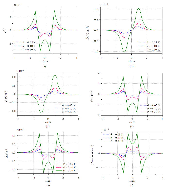
本节首先使用上节得到的各个区域物理场的解析表达式, 数值研究温度变化的大小对各个机电场的影响. 然后, 再用未作线性化处理的本构方程(4)在有限元软件COMSOL中进行模拟计算, 研究在温度变化稍大的情况下, 两个局部温度变化对压电半导体纤维杆的机电场及相应电学响应的影响. 作为数值算例, 我们以均匀掺杂的n型氧化锌(ZnO)半导体材料为例, 初始载流子密度为$n_{0}=10^{20}$ m$^{-3}$, 其弹性常数、压电常数和介电常数取自于文献[33], 热释电系数取自于文献[34], 热膨胀系数取自于文献[35],载流子迁移率取自于文献[36], 温度载荷作用位置为$a_{1}=a_{2}=b=0.6$ $\mu$m, 温度变化量为$\theta = \theta_{1}=-\theta_{2}=0.05$, 0.1和0.3 K ($\theta_{1}$与$\theta_{2}$分别为升温区域$a_{1}$与降温区域$a_{2}$的温度变化大小).图3给出了在不同温度改变下压电半导体杆中各物理量(电势、电位移、电极化、有效极化电荷密度、电子密度增量和总电荷密度)的分布情况. 可以看到随着温度改变量的增大, 各个物理场的变化也随之增大. 如果该结构是纯压电材材料, 那么各个物理场的分布会比较简单, 但由于压电半导体内载流子的屏蔽效应影响, 各个物理场会受到载流子重分布的影响而变得复杂. 图3(e)是结构中增量电子密度的分布情况, 表明了由于温度变化引起的热释电效应、热弹性与压电效应的耦合对压电电子学效应的影响. 需要注意的是, 由于模型中温度在界面$x=l_{1}$, $x=l_{2}$和$x=\pm b$处不连续, 造成了界面处有极化电荷的存在, 使得极化强度$P_{3}$在界面上不连续(如图3(c)所示). 文献[32]的结果表明, 一个局部的温度变化使杆中产生一个局部势垒和一个局部势阱, 从而阻碍压电半导体内载流子在外加电压下的定向移动, 给出了一种调控压电半导体内电荷运动的方法. 在这里, 升温和降温的两个局部温度变化使压电半导体杆体内产生了一个较大的势阱和分布在其两边的两个较小势垒(如图3(a)所示), 它具有类量子阱的特征. 可以看到势垒和势阱对温度的变化非常敏感, 随着温度变化量的增大, 势垒和势阱也随之变大. 需要指出的是: 由于图3(a)中给出的电势分布是线性化的解, 势垒势阱关于原点对称.
图3
 新窗口打开|下载原图ZIP|生成PPT
图3温度改变下各机电场 (a)电势$\varphi$; (b)电位移$D_{3}$; (c)电极化$P_{3}$; (d)有效极化电荷密度$\rho^P$; (e)电子密度增量$\Delta n$; (f)总电荷密度
Fig.3Distributions of (a) electric potential $\varphi$; (b) electric displacement $D_{3}$; (c) polarization $P_{3}$; (d) effective polarization charge density $\rho^P$; (e) electron concentration variation $\Delta n$; and (f) total charge for different temperature changes
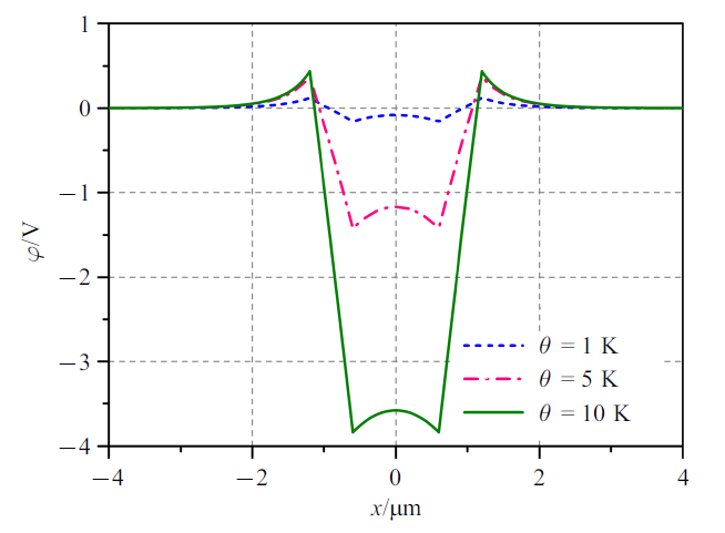
当温度变化量较大时, 上述线性化的解不再适用. 这里使用本构方程(4)中的非线性电流模型, 在COMSOL的PDE模块中对其进行数值模拟计算. 实际建模过程要求结构是有限长度的, 这里取杆长$2L=8.4$ $\mu$m. 初始载流子密度取为$n_{0}=10^{20}$ m$^{-3}$, 温度改变量$\theta =\theta_{1}=-\theta_{2}=1$, 5, 10 K. 我们主要关心由两个局部温度变化形成的势垒和势阱. 图4是电势在杆内的分布情况, 与图3(a)比较可以看到: 随着温度变化量的增大, 基于非线性和线性电流模型的计算结果的差别也越来越大. 图4显示随着温度变化量的增加, 势阱的深度逐渐变深, 这使得驱动电子定向运动"跃出"势阱所需的偏压增大; 而两边的势垒高度变化则相对不明显.
图4
 新窗口打开|下载原图ZIP|生成PPT
图4较大温度变化下压电半导体内电势$\varphi$分布
Fig.4Distributions of electric potential $\varphi$ under larger temperature changes
另外, 伏安特性曲线是压电半导体器件的一个重要参数. 下面, 我们在COMSOL中使用非线性的电流本构模型对此问题进行模拟计算. 同样, 考虑一根长为$2L=8.4$ $\mu$m, 初始载流子密度为$n_{0}=10^{20}$ m$^{-3}$, $a_{1}=a_{2}=a=b=0.6$ $\mu$m的氧化锌压电半导体杆. 杆的两端受到大小为2$V$的偏压, 电学边界条件如下
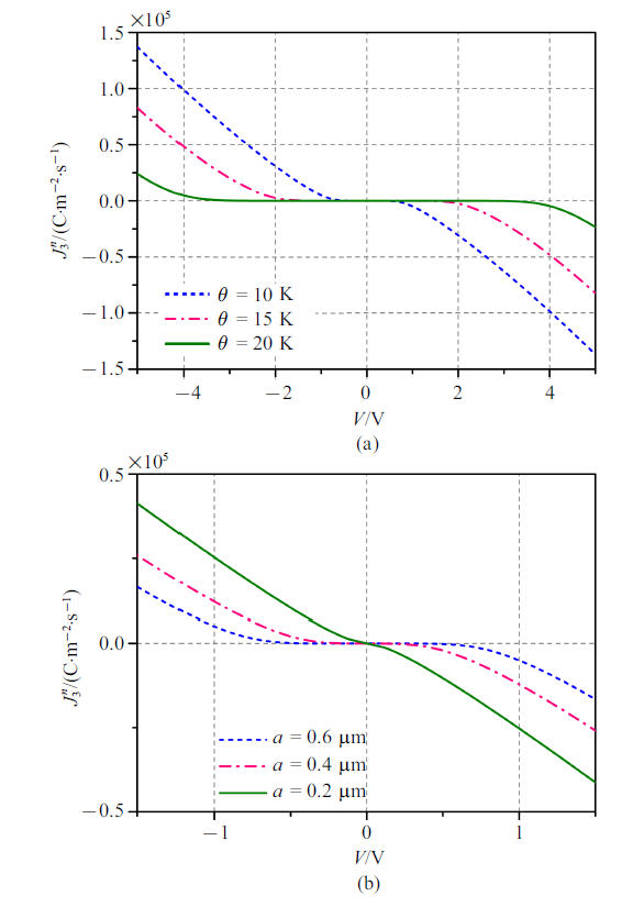
从图5(a)的$I$--$V$曲线中可以看到, 当升温区域$a_{1}$与降温区域$a_{2}$的温度改变量相同时, 即$\theta=\theta _{1}=-\theta _{2}=10$, 15, 20 K, 由温度改变形成的势垒/势阱阻碍了电子在外加偏压下的定向运动. 例如, 当$\theta =20$ K的曲线中, 外加偏压较小时(偏压小于2.5 V), 电子无法通过由温度变化形成的势垒/势阱区域而不能在电路中自由流通; 只有当外加偏压足够大时, 电子在外加偏压驱动下才能定向移动形成电流, 使电路导通. 这与文献[32]中单个局部温度变化的结果类似, 但需要指出: 文献[32]中由局部温度改变产生的势垒和势阱并不关于原点对称, 所以其能克服势垒/势阱使电路导通的正向偏压与反向偏压大小并不相同, 相应的$I$--$V$曲线也不关于原点反对称; 而由升温和降温两个区域形成的势垒和势阱, 在控制温度变化区域范围相同($a_{1}=a_{2}=a)$和温度改变也相同($\theta=\theta_{1}=-\theta_{2})$的条件下, 势垒和势阱关于原点对称, 为克服势垒和势阱作用而施加的正向和反向偏压大小相同, 这使得其$I$--$V$曲线关于原点反对称. 从图5(b)中可以看到, 保持上述各条件不变以及$\theta =10$ K, 仅减小温度载荷作用区域的范围(如由$a=0.6$ $\mu$m变化到$a=0.4$ $\mu$m和$a=0.2$ $\mu$m), 其$I$--$V$曲线依然关于原点反对称, 且在相同条件下, 温度变化区域的范围越大, 形成的势垒和势阱就越大, 使得在同样外加偏压情况下能通过的电子变少、电流减小.
图5
 新窗口打开|下载原图ZIP|生成PPT
图5压电半导体纤维杆的电学响应 (a)不同温度变化下的$I$--$V$曲线; (b) 温度变化区域大小变化下的$I$--$V$曲线
Fig.5Electrical behavior of piezoelectric semiconductor fiber (a) $I$--$V$ cures for different temperature changes; (b) $I$--$V$ cures for different length of $a$
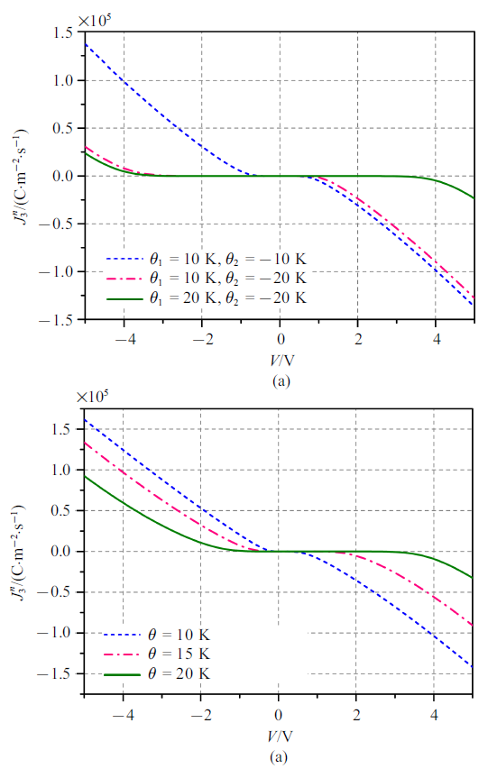
更为有意义的是: 通过合理确定压电半导体纤维杆受热载的区域和大小, 人为地打破势垒和势阱关于原点的对称性, 可以开发具有任意正向与反向导通偏压可编辑的电子器件. 图6(a)是两个局部温度变化区域范围相同($a_{1}=a_{2}=0.6$ $\mu$m), 但温度变化大小不同时的$I$--$V$曲线. 由图可知: 对于$\theta_{1}=10$ K和$\theta_{2}=-20$ K的情况, 由于升温和降温区温度变化量不同, 打破了$I$--$V$曲线的反对称性, 其正向偏压内的$I$--$V$曲线接近于$\theta_{1}=10$ K, $\theta_{2}=-10$ K情况下的$I$--$V$曲线; 其反向偏压内的$I$--$V$曲线则接近于$\theta_{1}=20$ K, $\theta_{2}=-20$ K情况下的$I$--$V$曲线. 这是因为外加正向偏压时, 为使电路导通, 需要克服主要由升温区域($\theta_{1}=10$ K)产生的势阱; 当外加反向偏压时, 为使电路导通, 需要克服主要由降温区域($\theta_{2}=-20$ K)产生的势阱. 图6(b)是保持升温和降温区温度变化 大小($\theta _1 =-\theta _2 =\theta $)不变、两个温度变化区域范围不同($a_{1}=0.6$ $\mu$m, $a_{2}=0.2$ $\mu$m)情况下的$I$--$V$曲线. 可以看到: 温度载荷作用区域的空间不对称性, 也打破了$I$--$V$曲线关于原点的反对称性. 当势垒或势阱关于原点对称时, 对于正负两个方向来说, 使载流子克服势垒/势阱作用在电路中流通所需的偏压大小相同, 此时压电半导体类似于一个正向和负向导通电压大小相同的温敏开关. 但人为地打破势垒和势阱关于原点的对称性, 可使正负两个方向的导通电压不再相同, 此时压电半导体将类似于一个二极管. 因此, 可以通过设计热载荷的大小和作用空间位置, 开发具有任意导通/击穿电压特性的类二极管温敏电子器件.
图6
 新窗口打开|下载原图ZIP|生成PPT
图6压电半导体纤维杆的电学响应 (a)升温与降温温区域温度改变不再相同下的$I$--$V$曲线; (b) 降温区域范围$a_{2}$变化下的$I$--$V$曲线
Fig.6Electrical behavior of piezoelectric semiconductor fiber (a) $I$--$V$ cures for different $\theta_{1}$ and $-\theta_{2}$; (b) $I$--$V$ cures for different length of $a_{2}$
4 结论
本文建立了压电半导体杆在多个局部温度载荷作用下的一维线性耦合力学模型. 压电半导体纤维杆在一个区域降温而在另一个区域升温的情况下, 两个局部温度改变对半导体杆内各物理量有显著影响; 在压电半导体内产生了两个局部势垒和一个局部势阱, 它使得部分载流子须在特定外加偏压下才能越过势垒或者跳出势阱进行定向移动. 势垒和势阱的大小取决于温度的改变量, 它决定了载流子在半导体内部的输运特性. 两局部温度载荷作用的空间位置和大小的不同, 均会打破其$I$--$V$曲线关于原点的反对称性. 因此, 可以实现基于压电半导体杆结构的温敏性电学开关功能. 本文研究结果为温敏型压电半导体电子学器件的开发与设计提供了理论指导.参考文献 原文顺序
文献年度倒序
文中引用次数倒序
被引期刊影响因子
URLPMID [本文引用: 1]
[本文引用: 2]
DOIURLPMID

Flexible piezotronic devices based on RF-sputtered piezoelectric semiconductor thin films have been investigated for the first time. The dominating role of the piezotronic effect over the geometrical and piezoresistive effect in the as-fabricated devices has been confirmed and the modulation effect of the piezopotential on charge carrier transport under different strains is subsequently studied. Moreover, it is also demonstrated that the UV sensing capability of the as-fabricated thin film based piezotronic device can be tuned by the piezopotential, showing significantly enhanced sensitivity and improved reset time under tensile strain.
DOIURLPMID [本文引用: 1]
Enhancing the output power of a nanogenerator is essential in applications as a sustainable power source for wireless sensors and microelectronics. We report here a novel approach that greatly enhances piezoelectric power generation by introducing a p-type polymer layer on a piezoelectric semiconducting thin film. Holes at the film surface greatly reduce the piezoelectric potential screening effect caused by free electrons in a piezoelectric semiconducting material. Furthermore, additional carriers from a conducting polymer and a shift in the Fermi level help in increasing the power output. Poly(3-hexylthiophene) (P3HT) was used as a p-type polymer on piezoelectric semiconducting zinc oxide (ZnO) thin film, and phenyl-C(61)-butyric acid methyl ester (PCBM) was added to P3HT to improve carrier transport. The ZnO/P3HT:PCBM-assembled piezoelectric power generator demonstrated 18-fold enhancement in the output voltage and tripled the current, relative to a power generator with ZnO only at a strain of 0.068%. The overall output power density exceeded 0.88 W/cm(3), and the average power conversion efficiency was up to 18%. This high power generation enabled red, green, and blue light-emitting diodes to turn on after only tens of times bending the generator. This approach offers a breakthrough in realizing a high-performance flexible piezoelectric energy harvester for self-powered electronics.
[本文引用: 1]
DOIURLPMID [本文引用: 1]
In this work we analyze the coupled piezoelectric and semiconductive behavior of vertically aligned ZnO nanowires under uniform compression. The screening effect on the piezoelectric field caused by the free carriers in vertically compressed zinc oxide nanowires (NWs) has been computed by means of both analytical considerations and finite element calculations. We predict that, for typical geometries and donor concentrations, the length of the NW does not significantly influence the maximum output piezopotential because the potential mainly drops across the tip, so that relatively short NWs can be sufficient for high-efficiency nanogenerators, which is an important result for wet-chemistry fabrication of low-cost, CMOS- or MEMS-compatible nanogenerators. Furthermore, simulations reveal that the dielectric surrounding the NW influences the output piezopotential, especially for low donor concentrations. Other parameters such as the applied force, the sectional area and the donor concentration have been varied in order to understand their effects on the output voltage of the nanogenerator.
DOIURLPMID [本文引用: 1]
The oscillating piezoelectric fields accompanying surface acoustic waves are able to transport charge carriers in semiconductor heterostructures. Here, we demonstrate high-frequency (above 1 GHz) acoustic charge transport in GaAs-based nanowires deposited on a piezoelectric substrate. The short wavelength of the acoustic modulation, smaller than the length of the nanowire, allows the trapping of photo-generated electrons and holes at the spatially separated energy minima and maxima of conduction and valence bands, respectively, and their transport along the nanowire with a well defined acoustic velocity towards indium-doped recombination centers.
DOIURLPMID [本文引用: 1]
Utilizing the coupled piezoelectric and semiconducting dual properties of ZnO, we demonstrate a piezoelectric field effect transistor (PE-FET) that is composed of a ZnO nanowire (NW) (or nanobelt) bridging across two Ohmic contacts, in which the source to drain current is controlled by the bending of the NW. A possible mechanism for the PE-FET is suggested to be associated with the carrier trapping effect and the creation of a charge depletion zone under elastic deformatioin. This PE-FET has been applied as a force/pressure sensor for measuring forces in the nanonewton range and even smaller with the use of smaller NWs. An almost linear relationship between the bending force and the conductance was found at small bending regions, demonstrating the principle of nanowire-based nanoforce and nanopressure sensors.
[本文引用: 1]
DOIURLPMID [本文引用: 1]
There has been significant interest in using electronically contacted nanorod or nanotube arrays as gas sensors, whereby an adsorbate modifies either the impedance or the Fermi level of the array, enabling detection. Typically, such arrays demonstrate the I-V curves of a Schottky diode that is formed using a metal-semiconductor junction with rectifying characteristics. We show in this work that nanostructured Schottky diodes have a functionally different response, characteristic of the large electric field induced by the size scale of the array. Specifically, they are characterized by a low reverse breakdown voltage. As a result, the reverse bias current becomes a strong function of the applied voltage. In this work, for the first time, we model this unique feature by describing the enhancement effect of high aspect ratio nanostructures on the I-V characteristics of a Schottky diode. A Pt/ZnO/SiC nanostructured Schottky diode is fabricated to verify the theoretical equations presented. The gas sensing properties of the Schottky diode in reversed bias is investigated and it is shown that the theoretical calculations are in excellent agreement with measurements.
[本文引用: 1]
[本文引用: 1]
[本文引用: 1]
DOIURLPMID [本文引用: 1]
The piezopotential in floating, homogeneous, quasi-1D piezo-semiconductive nanostructures under axial stress is an anti-symmetric (i.e., odd) function of force. Here, after introducing piezo-nano-devices with floating electrodes for maximum piezo-potential, we show that breaking the anti-symmetric nature of the piezopotential-force relation, for instance by using conical nanowires, can lead to better nanogenerators, piezotronic and piezophototronic devices.
[本文引用: 1]
[本文引用: 1]
DOIURL
DOIURLPMID
We have applied the perturbation theory for calculating the piezoelectric potential distribution in a nanowire (NW) as pushed by a lateral force at the tip. The analytical solution given under the first-order approximation produces a result that is within 6% from the full numerically calculated result using the finite element method. The calculation shows that the piezoelectric potential in the NW almost does not depend on the z-coordinate along the NW unless very close to the two ends, meaning that the NW can be approximately taken as a
DOIURLPMID
We have investigated the behavior of free charge carriers in a bent piezoelectric semiconductive nanowire under thermodynamic equilibrium conditions. For a laterally bent n-type ZnO nanowire, with the stretched side exhibiting positive piezoelectric potential and the compressed side negative piezoelectric potential, the conduction band electrons tend to accumulate at the positive side. The positive side is thus partially screened by free charge carriers while the negative side of the piezoelectric potential preserves as long as the donor concentration is not too high. For a typical ZnO nanowire with diameter 50 nm, length 600 nm, donor concentration N(D) = 1 x 10(17) cm(-3) under a bending force of 80 nN, the potential in the positive side is <0.05 V and is approximately -0.3 V at the negative side. The theoretical results support the mechanism proposed for a piezoelectric nanogenerator. Degeneracy in the positive side of the nanowire is significant, but the temperature dependence of the potential profile is weak for the temperature range of 100-400 K.
[本文引用: 1]
[本文引用: 1]
[本文引用: 2]
URLPMID [本文引用: 1]
[本文引用: 7]
[本文引用: 1]
[本文引用: 1]
[本文引用: 1]
[本文引用: 1]
