 ,21 Department of Information and Technology,
 2 State Key Laboratory of Electronic Thin Films and Integrated Devices,
Received:2020-02-25Revised:2020-06-21Accepted:2020-06-24Online:2020-10-15
| Fund supported: |

Abstract
Keywords:
PDF (1538KB)MetadataMetricsRelated articlesExportEndNote|Ris|BibtexFavorite
Cite this article
Xiao-Zhen Li(李小珍), Meng-Jiang Xing(邢孟江). Mechanical anisotropy and electronic properties of X2N2 (XH2 ): first-principles calculations
1. Introduction
Group 14 elements have a variety of allotropes [1 –10] and their own alloy materials [11 –16]. At the same time, the group 14 elements (C, Si, Ge) can form a variety of compounds [17 –26]. The new carbon-nitride-related material C2 N2 (CH2 ) has been investigated in recently year, and C2 N2 (CH2 ) in Cmc 21 space group has been synthesized by Sougawa et al [17]. The C2 N3 H in Cmc 21 phase proposed by Salamat et al [18] has a bulk modulus equivalent to that of high hardness silicon nitride ceramics. Later, Sougawa et al [19] studied the change of structure and bulk modulus of this structure under high pressure. They found that the strength of carbon–nitrogen single bond is the same as that of carbon–carbon single bond in diamond. Then, Takarabe et al [20] investigated the electronic band structures of IV2 V2 VI class semiconductors, C2 N2 O, C2 N2 NH, C2 N2 CH2 used the screened-exchange local density approximation (sX-LDA) [27] by first-principles calculations, the valence of X atom is actually two, so the substitution of X (X quarter O, NH, CH2 ) is isoelectronic. They found that the upper VB (valence band) is dominated by N 2p and X 2p orbits, and the calculated absorption edge moves to the low energy direction as the substituent shifts from O atom to CH2 group. The structural properties, mechanical properties, electronic properties and thermodynamic properties of C2 N2 (CH2 ) are study used first-principles calculations by Wei et al [21], C2 N2 (CH2 ) has a large bulk modulus and shear modulus, and it is a kind of potential incompressible hard material. In addition, the maximum value of Young’s modulus of C2 N2 (CH2 ) is along the [001] direction. In the pressure range of 0–100 GPa and 0–2000 K, the thermodynamic properties, such as heat capacity, thermal expansion, and Grüneisen parameters of C2 N2 (CH2 ) were investigated by the quasi harmonic Debye model. Very Recently, Arrerut et al [22] investigated the physical properties under high pressure, in the pressure range of 50 GPa, the band gap within GGA level decreases at the rate of 7.5 meV GPa−1 .The two novel silicon-nitride-related material Si2 N2 (SiH2 ), and germanium-nitride-related material Ge2 N2 (GeH2 ) are proposed by the first principle method, and their stability is proved. In the present work, using first-principles calculations, the electronic band structures, structural properties, mechanical anisotropy, and thermal properties of C2 N2 (CH2 ), Si2 N2 (SiH2 ) and Ge2 N2 (GeH2 ) are detailed investigated in this work.
2. Computational detail
This work utilized the Cambridge Serial Total Energy Package plane-wave code [28] based on density functional theory [29, 30]. The structural optimization utilized the Broyden–Fletcher–Goldfarb–Shanno [31] minimization. The interactions between the ionic core and valence electrons were described by the ultrasoft pseudopotential [32] for calculating the elastic properties and structural optimizations in this work. The exchange correlation potential was performed with the LDA [33, 34] and generalized gradient approximation in the form of the Perdew–Burke–Ernzerhof function [35]. For calculating the elastic properties and structural optimizations, a plane wave cut-off energy of 500 eV was adopted. The high Monkhorst–Pack [36] points less than or about 2π ×0.025 Å−1 for the conventional cells of C2 N2 (CH2 ), Si2 N2 (SiH2 ), and Ge2 N2 (GeH2 ), in other words, 5×9×10 in the Brillouin zone for C2 N2 (CH2 ); 3×7×8 for Si2 N2 (SiH2 ), 3×7×8 for Ge2 N2 (GeH2 ), respectively. For the electronic band structures, the Heyd–Scuseria–Ernzerhof (HSE06) hybrid functional [37] are adopted for sufficiently accurate calculations of the electronic band structures of X2 N2 (XH2 ) (X=C, Si, Ge). In addition, the phonon spectra of X2 N2 (XH2 ) are determined using the linear response approach, called the density functional perturbation theory [38].3. Results and discussion
3.1. Structural properties
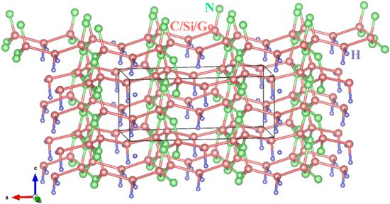
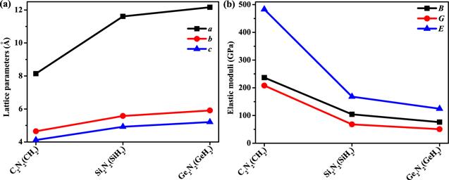
The crystal structures of X2 N2 (XH2 ) (X=C, Si, Ge) are shown in figure 1, here, the dark pink, green and purple spheres represent the X atoms (X=C, Si, Ge), N atoms and H atoms, respectively. The optimized lattice constants of X2 N2 (XH2 ) (X=C, Si, Ge) are listed in table 1 . The C2 N2 (CH2 ) has been synthesized experimentally by Sougawa et al [17], Si2 N2 (SiH2 ) and Ge2 N2 (GeH2 ) are first proposed in this work. The lattice parameters of X2 N2 (XH2 ) increase with the X atoms form carbon, silicon to germanium atom, the fastest growing direction is direction a . Because there are more silicon–silicon bonds in this direction, and the silicon–silicon bond length (Si–Si: bond length: 2.367 35 Å) increases more than the carbon–carbon bond (C–C bond length: 1.553 38 Å), and the silicon–nitrogen bond length (Si–N bond length: 1.761 53 Å) increases less than the carbon–nitrogen bond (C–N bond length: 1.506 54 Å). When X atom changes from carbon atom to silicon atom and then to germanium atom, the lattice parameter a increases the most, 49.46% more than C2 N2 (CH2 ), and the lattice parameter c increases the least, 26.58% more than C2 N2 (CH2 ).Figure 1.
 New window|Download| PPT slide
Figure 1.The crystal structures of X2 N2 (XH2 ) (X=C, Si, Ge).
Table 1.
Table 1.The calculated lattice parameters (Å) of X2 N2 (XH2 ) (X=C, Si, Ge) with different functionals.
| a | b | c | V | ||
|---|---|---|---|---|---|
| C2 N2 (CH2 ) | GGA | 8.1403 | 4.6462 | 4.1162 | 155.680 |
| LDA | 8.0061 | 4.5658 | 4.0656 | ||
| sX-LDA | 8.1222 | 4.4630 | 4.1177 | ||
| Experimental | 7.6250 | 4.4900 | 4.0470 | ||
| Si2 N2 (SiH2 ) | GGA | 11.6131 | 5.5769 | 4.9216 | 318.748 |
| LDA | 11.3936 | 5.4473 | 4.8228 | 299.326 | |
| Ge2 N2 (GeH2 ) | GGA | 12.1665 | 5.9103 | 5.2103 | 374.663 |
| LDA | 11.7703 | 5.6907 | 5.0368 | 337.376 |
New window|CSV
3.2. Stability
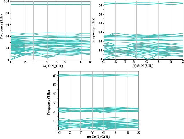
Although C2 N2 (CH2 ) has been synthesized, the phonon spectrum of C2 N2 (CH2 ) is given in previous work [21]. The phonon spectra of Si2 N2 (SiH2 ) and Ge2 N2 (GeH2 ) are shown in figures 3 (a) and (b), respectively. There is no curve below zero in the phonon spectrum, which proves that the material is dynamically stable. In other words, all the C2 N2 (CH2 ), Si2 N2 (SiH2 ) and Ge2 N2 (GeH2 ) are dynamically stable. The elastic constants and elastic moduli of X2 N2 (XH2 ) are listed in table 2 . The all space group of X2 N2 (XH2 ) is Cmc 21, it belongs the orthorhombic symmetry. For orthogonal systems, the necessary and sufficient born criteria: C11 >0, C44 >0, C55 >0, C66 >0, C11C22 >Table 2.
Table 2.The elastic constants (GPa) and elastic modulus (GPa) of X2 N2 (XH2 ) (X=C, Si, Ge).
| C11 | C22 | C33 | C44 | C55 | C66 | C12 | C13 | C23 | B | G | E | ||
|---|---|---|---|---|---|---|---|---|---|---|---|---|---|
| C2 N2 (CH2 ) | GGA | 471 | 464 | 712 | 275 | 186 | 150 | 53 | 116 | 104 | 237 | 208 | 483 |
| GGA | 505 | 489 | 728 | 283 | 186 | 143 | 85 | 122 | 99 | 256 | 210 | 494 | |
| LDA | 554 | 547 | 794 | 308 | 212 | 170 | 104 | 137 | 120 | 286 | 234 | 552 | |
| LDA | 529 | 510 | 799 | 309 | 201 | 145 | 77 | 142 | 119 | 272 | 222 | 524 | |
| Si2 N2 (SiH2 ) | GGA | 199 | 200 | 240 | 104 | 50 | 43 | 58 | 45 | 48 | 104 | 68 | 167 |
| LDA | 218 | 176 | 257 | 114 | 51 | 42 | 51 | 63 | 59 | 109 | 69 | 171 | |
| Ge2 N2 (GeH2 ) | GGA | 137 | 146 | 182 | 74 | 37 | 36 | 44 | 34 | 33 | 76 | 51 | 125 |
| LDA | 198 | 114 | 152 | 88 | 34 | 57 | 39 | 25 | 13 | 67 | 58 | 135 |
New window|CSV
Figure 2.
 New window|Download| PPT slide
Figure 2.The lattice parameters (a) and elastic modulus (b) of X2 N2 (XH2 ) (X=C, Si, Ge), respectively.
Figure 3.
 New window|Download| PPT slide
Figure 3.The phonon spectra of C2 N2 (CH2 ) (a), Si2 N2 (SiH2 ) (b) and Ge2 N2 (GeH2 ) (c), respectively.
Figure 4.
 New window|Download| PPT slide
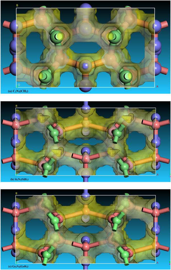
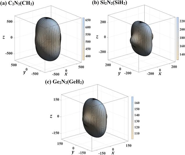
Figure 4.The electron localization function (ELF) distribution of C2 N2 (CH2 ), Si2 N2 (SiH2 ) and Ge2 N2 (GeH2 ) with an isovalue of 0.75.
3.3. Electronic properties
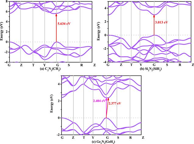
The electronic band structures of C2 N2 (CH2 ), Si2 N2 (SiH2 ) and Ge2 N2 (GeH2 ) with HSE06 hybrid functional are shown in figures 5 (a)–(c), respectively. From the figure 5, it is clear that the Ge2 N2 (GeH2 ) is quasi-direct band gap semiconductor materials, while the C2 N2 (CH2 ) and Si2 N2 (SiH2 ) both are direct band gap semiconductor material. The difference of direct band gap and indirect band gap of Ge2 N2 (GeH2 ) is only 0.027 eV. For C2 N2 (CH2 ) and Si2 N2 (SiH2 ), the valence band maximum (VBM) and conduction band minimum (CBM) both located at the G point (also called Γ point), the VBM of Ge2 N2 (GeH2 ) also located at the G point, while the CBM of Ge2 N2 (GeH2 ) located between the G point and S (0.0 0.5 0.0). The Fermi level of X2 N2 (XH2 ) are also investigated in this work, the Fermi level of C2 N2 (CH2 ), Si2 N2 (SiH2 ) and Ge2 N2 (GeH2 ) is 8.231 eV, 0.225 eV and −1.449 eV. As X atoms changes from carbon atoms to silicon atoms and then to germanium atoms, the Fermi energy level of X2 N2 (XH2 ) decreases straight forward. The wide band gap and direct band gap imply that of C2 N2 (CH2 ), Si2 N2 (SiH2 ) and Ge2 N2 (GeH2 ) can be good semiconductor material and optical material. If group 14 of C2 N2 (CH2 ), Si2 N2 (SiH2 ) and Ge2 N2 (GeH2 ) are doped (such as C2−x Six N2 (CH2 ), C2 N2 (C1−x Six H2 ), or Si2−x Gex N2 (SiH2 ), and soon on), their band gap may be adjusted between 2.377 and 5.634 eV.Figure 5.
 New window|Download| PPT slide
Figure 5.The electronic band structures of C2 N2 (CH2 ) (a), Si2 N2 (SiH2 ) (b), and Ge2 N2 (GeH2 ) (c), respectively.
3.4. Debye temperature
The Debye temperature is another important physical quantity reflecting the bonding force between atoms. The Debye temperature of different materials is different, and the melting point is high; that is to say, the stronger the bonding force of atoms is, the higher the Debye temperature is. The Debye temperature, the compressional sound velocity vp and shear sound velocity vs, the average sound velocity vm of C2 N2 (CH2 ), Si2 N2 (SiH2 ) and Ge2 N2 (GeH2 ) are shown in table 3 . The detailed calculation formula appears in [39]. From table 3, the compressional sound velocity vp and shear sound velocity vs, the average sound velocity vm of C2 N2 (CH2 ), Si2 N2 (SiH2 ) and Ge2 N2 (GeH2 ) decreases with the X atoms from C to Si, to Ge atoms. The decrease of average sound velocity vm is the fastest, the effective rate of compressional sound velocity vp is only next to vm, which is 57.62%, it is slightly less than 60.06% of average sound velocity vm, and the decrease of the shear sound velocity vs is the slowest, which is 37.79%. The Debye temperature of C2 N2 (CH2 ) is 1589 K, which is the greatest in X2 N2 (XH2 ), and slightly smaller than that of o P8-B2 CO (1687 K), t I16-B2 CO (1718 K) and t P4-B2 CO (1645 K). In addition, the Debye temperature of X2 N2 (XH2 ) reduced by 70.17%.Table 3.
Table 3.The calculated density (g cm−3 ), the longitudinal, transverse and mean wave velocity (vs, vp, vm in m s−1 ), and the Debye temperature (K) for X2 N2 (XH2 ) (X=C, Si, Ge).
| ρ | vp | vs | vm | ΘD | |
|---|---|---|---|---|---|
| C2 N2 (CH2 ) | 2.8186 | 13 508 | 8590 | 9445 | 1589 |
| Si2 N2 (SiH2 ) | 2.3815 | 9041 | 5344 | 5920 | 849 |
| Ge2 N2 (GeH2 ) | 4.3931 | 5725 | 3407 | 3772 | 474 |
New window|CSV
3.5. Mechanical anisotropy properties
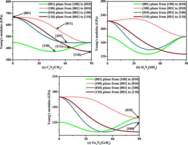
The mechanical anisotropy of C2 N2 (CH2 ), Si2 N2 (SiH2 ) and Ge2 N2 (GeH2 ) in Young’s modulus, shear modulus and Poisson’s ratio are systematic investigated in this work. First, we focus on Young’s modulus. The three-dimensional surface constructions of Young’s modulus for X2 N2 (XH2 ) are estimated by elastic anisotropy measures code [40], the related results are shown in figure 6 . As we all know, the three-dimensional surface constructions of Young’s modulus of isotropic materials is a hollow sphere, and any three-dimensional surface constructions of Young’s modulus without hollow sphere can be considered as anisotropic [28]. Some researches have also successfully used this method to predict its mechanical anisotropy [16, 41 –47]. From figure 6, the shape of the three-dimensional surface constructions of C2 N2 (CH2 ), Si2 N2 (SiH2 ) and Ge2 N2 (GeH2 ) exhibits the mechanical anisotropy. The values of Young’s moduli of C2 N2 (CH2 ) and Si2 N2 (SiH2 ) are the same in x -axis and y -axis, while the values of Young’s modulus of Ge2 N2 (GeH2 ) in x -axis (120 GPa) is less than that of y -axis (129 GPa). From the shape of the three-dimensional surface constructions of C2 N2 (CH2 ), Si2 N2 (SiH2 ) and Ge2 N2 (GeH2 ), the Young’s modulus in x -axis of Si2 N2 (SiH2 ) deviates a lot from that in z -axis, the Ez /Ex =229/118=1.94, it is much greater than that of C2 N2 (CH2 ) (Ez /Ex =665/449=1.48) and Ge2 N2 (GeH2 ) (Ez /Ex =170/120=1.42, Ez /Ey =170/129=1.32). It also shows that Young’s modulus is mechanical anisotropic on C2 N2 (CH2 ), Si2 N2 (SiH2 ) and Ge2 N2 (GeH2 ).Figure 6.
 New window|Download| PPT slide
Figure 6.The directional dependence of Young’s modulus of C2 N2 (CH2 ) (a), Si2 N2 (SiH2 ) (b), and Ge2 N2 (GeH2 ) (c), respectively.
In order to study the anisotropy of Young’s modulus more systematically, the distribution of Young’s modulus in three main planes was also studied in this work. The maximum values, the minimum values and Emax /Emin ratio of Young’s modulus of X2 N2 (XH2 ) are listed in table 4, and the maximum values, the minimum values, and Emax /Emin ratio of Young’s modulus of in (001) plane, (010) plane and (100) plane are listed in table 5 . The maximum values of C2 N2 (CH2 ), Si2 N2 (SiH2 ) and Ge2 N2 (GeH2 ) are 665 GPa, 229 GPa, and 170 GPa, respectively, and the minimum values of C2 N2 (CH2 ), Si2 N2 (SiH2 ) and Ge2 N2 (GeH2 ) are 372 GPa, 127 GPa, and 101 GPa, respectively. From tables 4 and 5, one can see that only the maximum values of Young’s modulus of C2 N2 (CH2 ), Si2 N2 (SiH2 ), and Ge2 N2 (GeH2 ) appear in (100) plane, and only the maximum values and the minimum values of Ge2 N2 (GeH2 ) both appear in (010) plane. Therefore, the anisotropy of Young’s modulus in the three main planes is not as good as that of the whole material, except for (010) plane of Ge2 N2 (GeH2 ). For these three main planes, Young’s modulus shows the largest mechanical anisotropy in (010) plane.
Table 4.
Table 4.The calculated the maximum values, the minimum values, and ratio of Young’s modulus, shear modulus and Poisson’s ratio of X2 N2 (XH2 ) (X=C, Si, Ge).
| E | G | v | |||||||
|---|---|---|---|---|---|---|---|---|---|
| Emax | Emin | Ratio | Gmax | Gmin | Ratio | vmax | vmin | Ratio | |
| C2 N2 (CH2 ) | 665 | 372 | 1.79 | 275 | 150 | 1.83 | 0.29 | 0.07 | 4.14 |
| Si2 N2 (SiH2 ) | 229 | 127 | 1.80 | 104 | 43 | 2.42 | 0.48 | 0.07 | 6.86 |
| Ge2 N2 (GeH2 ) | 170 | 101 | 1.68 | 74 | 36 | 2.05 | 0.42 | 0.07 | 6.00 |
New window|CSV
Table 5.
Table 5.The calculated the maximum values, the minimum values, and ratio of Young’s modulus, shear modulus and Poisson’s ratio of X2 N2 (XH2 ) (X=C, Si, Ge) in (100) plane, (010) plane, and (001) plane.
| (100) plane | (010) plane | (001) plane | |||||||
|---|---|---|---|---|---|---|---|---|---|
| Emax | Emin | Ratio | Emax | Emin | Ratio | Emax | Emin | Ratio | |
| C2 N2 (CH2 ) | 665 | 446 | 1.49 | 665 | 446 | 1.49 | 449 | 372 | 1.21 |
| Si2 N2 (SiH2 ) | 229 | 178 | 1.29 | 223 | 140 | 1.59 | 178 | 127 | 1.40 |
| Ge2 N2 (GeH2 ) | 170 | 129 | 1.32 | 170 | 101 | 1.68 | 129 | 102 | 1.27 |
| (100) plane | (010) plane | (001) plane | |||||||
| Gmax | Gmin | Ratio | Gmax | Gmin | Ratio | Gmax | Gmin | Ratio | |
| C2 N2 (CH2 ) | 275 | 150 | 1.83 | 275 | 150 | 1.83 | 275 | 150 | 1.83 |
| Si2 N2 (SiH2 ) | 104 | 43 | 2.42 | 104 | 43 | 2.42 | 104 | 43 | 2.42 |
| Ge2 N2 (GeH2 ) | 74 | 36 | 2.06 | 74 | 36 | 2.06 | 74 | 36 | 2.06 |
| (100) plane | (010) plane | (001) plane | |||||||
| vmax | vmin | Ratio | vmax | vmin | Ratio | vmax | vmin | Ratio | |
| C2 N2 (CH2 ) | 0.22 | 0.07 | 3.14 | 0.28 | 0.08 | 3.50 | 0.24 | 0.08 | 3.00 |
| Si2 N2 (SiH2 ) | 0.26 | 0.07 | 3.71 | 0.40 | 0.19 | 2.11 | 0.47 | 0.10 | 4.70 |
| Ge2 N2 (GeH2 ) | 0.29 | 0.07 | 4.14 | 0.39 | 0.14 | 2.76 | 0.41 | 0.11 | 3.73 |
New window|CSV
Furthermore, we study the magnitude of Young’s modulus of C2 N2 (CH2 ), Si2 N2 (SiH2 ) and Ge2 N2 (GeH2 ) in different directions on the main plane. When the Young’s modulus of the tensile axis is in the (001) plane, let α be the angle of between [hk 0] and [100], the orientation dependence of Young’s modulus of C2 N2 (CH2 ), Si2 N2 (SiH2 ) and Ge2 N2 (GeH2 ) can be expressed as follows [21]: E−1 =s11 cos4α +s22 sin4α + 2s12 sin2α cos2α +s66 sin2α cos2α . For (100) plane, let β be the angle of between [001] and [0kl ], the orientation dependence of X2 N2 (XH2 ) can be expressed as follows: E−1 =s22 sin4β + s33 cos4β +(s23 sin2 2β)/2+(s44 sin2 2β)/4. For (010) plane, let γ be the angle of between [001] and [h 0l ], the orientation dependence of X2 N2 (XH2 ) can be expressed as follows: E−1 = s11 sin4γ +s33 cos4γ +(s13 sin2 2γ)/2+(s55 sin2 2β)/4. For (1-10) plane, let δ be the angle of between [001] and [hkl ], the orientation dependence of X2 N2 (XH2 ) can be expressed as follows: E−1 =[sin4δ /(a2 +b2 )2 ][a4s11 +b4s12 +a2b2 (2s12 +s66 )] + s33 cos4δ +[sin2δ cos2δ /(a2 +b2 )][a2 (2s13 +s55 )+b2 (2s23 + s44 )]. The related results of orientation dependence of X2 N2 (XH2 ) are illustrated in figure 7 . The greatest value and the smallest value of Young’s modulus of C2 N2 (CH2 ) is 665 GPa and 372 GPa when the tensile axis is along [001] direction and along [120] direction, respectively, it is much closed the previous report (686 and 376 GPa) [5]. When the tensile axis is in a particular direction, the order of the Young’s modulus of Si2 N2 (SiH2 ): E[110] <E[120] <E[111] <E[101] <E[010] = E[100] <E[011] <E[001], and the order of the Young’s modulus of Ge2 N2 (GeH2 ): E[110] <E[111] <E[101] <E[120] <E[100] < E[010] <E[011] <E[001] . The order of Young’s modulus of Si2 N2 (SiH2 ) and Ge2 N2 (GeH2 ) in different directions is different from that of C2 N2 (CH2 ).
Figure 7.
 New window|Download| PPT slide
Figure 7.Orientation dependence of Young’s modulus of C2 N2 (CH2 ) (a), Si2 N2 (SiH2 ) (b), and Ge2 N2 (GeH2 ) (c), respectively.
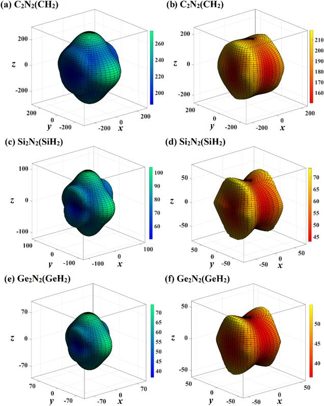
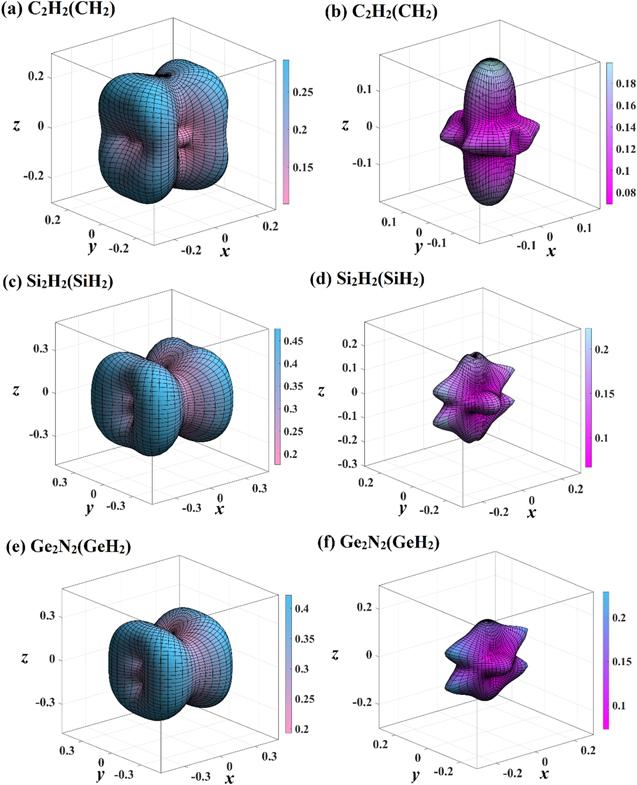
The three-dimensional surface constructions of the maximum values and the minimum values of shear modulus and Poisson’s ratio in different directions of X2 N2 (XH2 ) are displayed in figure 8 and 9, respectively. For shear modulus, the blue green surface constructions represents the maximum values surface construction, and red yellow surface constructions represents the minimum values surface construction. For Poisson’s ratio, the light blue pink surface constructions and light blue purple surface constructions represents the maximum values surface construction and the minimum values surface construction, respectively. From the shapes of three-dimensional surface constructions of shear modulus and Poisson’s ratio of X2 N2 (XH2 ), one can see that the C2 N2 (CH2 ), Si2 N2 (SiH2 ) and Ge2 N2 (GeH2 ) also exhibits mechanical anisotropy in shear modulus and Poisson’s ratio. The maximum values, the minimum values and Gmax /Gmin ratio of shear modulus of X2 N2 (XH2 ) are also listed in table 5, and the maximum values, the minimum values, and vmax /vmin ratio of Poisson’s ratio of in (001) plane, (010) plane and (100) plane are also listed in table 5 . Unlike Poisson’s ratio and Young’s modulus, only the maximum and minimum of shear modulus of X2 N2 (XH2 ) appear in three main planes, (001) plane, (010) plane and (100) plane. In addition, the mechanical anisotropy in shear modulus of Si2 N2 (SiH2 ) and Ge2 N2 (GeH2 ) are both slightly greater than that of C2 N2 (CH2 ), and the mechanical anisotropy in shear modulus of Si2 N2 (SiH2 ) is the greatest. For Poisson’s ratio, similar to Young’s modulus, only the minimum values of Poisson’s ratio of X2 N2 (XH2 ) appears in three main planes. The mechanical anisotropy in Poisson’s ratio of Si2 N2 (SiH2 ) is the greatest. For three main planes, the mechanical anisotropy in Poisson’s ratio in (001) plane of Si2 N2 (SiH2 ) is the greatest, while mechanical anisotropy in Poisson’s ratio in (010) plane of Si2 N2 (SiH2 ) is the smallest. The (010) plane and (001) plane of C2 N2 (CH2 ) exhibits the greatest and smallest mechanical anisotropy in Poisson’s ratio, respectively. While (100) plane and (010) plane of Ge2 N2 (GeH2 ) exhibits the greatest mechanical anisotropy in Poisson’s ratio, respectively.
Figure 8.
 New window|Download| PPT slide
Figure 8.The directional dependence of shear modulus of C2 N2 (CH2 ) (a), (b), Si2 N2 (SiH2 ) (c), (d), and Ge2 N2 (GeH2 ) (e), (f), respectively. The blue green three-dimensional surface constructions represent the maximum values of shear modulus, and the red yellow surface constructions represent the minimum values of shear modulus, respectively.
Figure 9.
 New window|Download| PPT slide
Figure 9.The directional dependence of Poisson’s ratio of C2 N2 (CH2 ) (a), (b), Si2 N2 (SiH2 ) (c), (d), and Ge2 N2 (GeH2 ) (e), (f), respectively. The light blue pink three-dimensional surface constructions represent the maximum values of Poisson’s ratio, and the light blue purple surface constructions represent the minimum values of Poisson’s ratio, respectively.
4. Conclusion
The novel silicon nitride phase Si2 N2 (SiH2 ) and novel germanium nitride phase Ge2 N2 (GeH2 ) in Cmc 21 structure are proposed in this work. Then, the structural, mechanical anisotropy, electronic band structures and thermal properties of C2 N2 (CH2 ), Si2 N2 (SiH2 ) and Ge2 N2 (GeH2 ) are detailed investigated in this work. First, their stability has been confirmed by phonon spectrum and elastic constants. Secondly, the electronic band calculation of hybrid functional shows that C2 N2 (CH2 ), Si2 N2 (SiH2 ) and Ge2 N2 (GeH2 ) are all wide band gap semiconductor materials, and C2 N2 (CH2 ) and Si2 N2 (SiH2 ) are direct band gap semiconductor materials, while silicon is a quasi-direct band gap semiconductor material. The wide band gap and direct band gap imply that of C2 N2 (CH2 ), Si2 N2 (SiH2 ) and Ge2 N2 (GeH2 ) can be good semiconductor material and optical material. The Debye temperature of C2 N2 (CH2 ), Si2 N2 (SiH2 ) and Ge2 N2 (GeH2 ) is 1589 K, 849 K and 474 K, respectively. Then, the three-dimensional surface constructions of Young’s modulus, shear modulus and Poisson’s ratio of C2 N2 (CH2 ), Si2 N2 (SiH2 ) and Ge2 N2 (GeH2 ) all shows the different levels mechanical anisotropy. For these (100), (010), (001) planes, Young’s modulus shows the largest mechanical anisotropy in (010) plane. For Poisson’s ratio, the (010) plane of C2 N2 (CH2 ) shows the largest mechanical anisotropy, the (001) plane of Si2 N2 (SiH2 ) illustrates the largest mechanical anisotropy, the (100) plane of Ge2 N2 (GeH2 ) illustrates the largest mechanical anisotropy. While the shear modulus of C2 N2 (CH2 ), Si2 N2 (SiH2 ) and Ge2 N2 (GeH2 ) are all mechanical isotropy in (100), (010), (001) planes.Acknowledgments
This work was funded by the National Natural Science Foundation of China (grant numbers 61864004 and 61564005).Reference By original order
By published year
By cited within times
By Impact factor
DOI:10.1016/j.diamond.2020.107831 [Cited within: 1]
DOI:10.1016/j.matchemphys.2019.122480
DOI:10.1016/j.commatsci.2020.109634
DOI:10.3390/ma13081926
DOI:10.1103/PhysRevLett.118.245701 [Cited within: 1]
DOI:10.1039/C6CP00195E
DOI:10.1002/cphc.201800903
DOI:10.1103/PhysRevLett.121.175701
DOI:10.3390/ma13092079
DOI:10.1088/0253-6102/71/8/1036 [Cited within: 1]
DOI:10.1007/s10853-018-2249-9 [Cited within: 1]
DOI:10.1063/1.5095203
DOI:10.1088/1361-648X/ab11a2
DOI:10.1088/0253-6102/68/2/259
DOI:10.1007/s10853-017-1681-6
DOI:10.1016/j.cap.2019.08.019 [Cited within: 2]
DOI:10.1143/JJAP.50.095503 [Cited within: 4]
DOI:10.1103/PhysRevB.80.104106 [Cited within: 1]
DOI:10.1063/1.4789020 [Cited within: 1]
DOI:10.1063/1.4731749 [Cited within: 1]
DOI:10.1016/j.chemphys.2013.02.015 [Cited within: 4]
DOI:10.1021/acs.jpcc.7b06594 [Cited within: 1]
DOI:10.1016/j.jssc.2011.01.004
DOI:10.1002/pssb.201248225
DOI:10.3390/ma9050333
DOI:10.3390/ma12213589 [Cited within: 1]
DOI:10.1103/PhysRevB.53.3764 [Cited within: 1]
DOI:10.1016/j.commatsci.2013.10.029 [Cited within: 2]
DOI:10.1103/PhysRev.136.B864 [Cited within: 1]
DOI:10.1103/PhysRev.140.A1133 [Cited within: 1]
DOI:10.1006/jcph.1996.5612 [Cited within: 1]
DOI:10.1103/PhysRevB.41.7892 [Cited within: 1]
DOI:10.1103/PhysRevLett.45.566 [Cited within: 1]
DOI:10.1103/PhysRevB.23.5048 [Cited within: 1]
DOI:10.1103/PhysRevLett.77.3865 [Cited within: 1]
DOI:10.1103/PhysRevB.13.5188 [Cited within: 1]
DOI:10.1063/1.1564060 [Cited within: 1]
DOI:10.1103/RevModPhys.73.515 [Cited within: 1]
DOI:10.1016/j.jssc.2018.12.012 [Cited within: 1]
DOI:10.1016/j.cpc.2010.08.033 [Cited within: 1]
DOI:10.1088/1674-1056/28/3/036101 [Cited within: 1]
DOI:10.3390/ma13061280
DOI:10.3390/ma10121413
DOI:10.1016/j.commatsci.2018.11.004
DOI:10.1016/j.jpcs.2014.12.008
DOI:10.1088/1361-648X/ab8982
DOI:10.1088/1361-6641/ab76ae [Cited within: 1]
