Key Laboratory for Special Fiber and Fiber Sensor of Hebei Province, School of Information Science and Engineering, Yanshan University, Qinhuangdao 066004, China
Fund Project:Project supported by the National Key R&D Program of China (Grant Nos. 2019YFC1407900, 2017YFC1403800), the Key Program of the National Natural Science Foundation of China (Grant No. 61735011), and the Key Research and Development Planning Project of Hebei Province, China (Grant No. 18273302D)
Received Date:18 May 2020
Accepted Date:17 June 2020
Available Online:29 September 2020
Published Online:05 October 2020
Abstract:The integration of fiber with graphene has greatly expanded the two-dimensional functional materials in the field of photonics research. However, the growth method by using chemical vapor deposition with metal catalytic substrateis limited to the fabrication of a graphene-fiber composite due to inevitably transferring graphene flakes onto the optical fiber surface. In order to fully achieve the interaction between light and graphene material, optical fibers have to be treated with special structure, which greatly damages the fiber structure, resulting in inefficient and harmful manufacturing strategy for the mass production. In this paper, a graphene-photonic crystal fiber (G-PCF) composite is prepared by atmospheric chemical vapor deposition (APCVD), which can directly grow monolayer and multi-layer graphene into the air-hole of photonic crystal fiber. Furthermore, we randomly break a G-PCF and then conduct an electron microscope (SEM) test at the fractured section. It is obvious that a tube-like graphene protruding out of one hole in the fractured area of the G-PCF is observed, thus further demonstrating that a monolayer graphene is grown on the inner hole walls of the PCF as shown in Fig. 2. By changing the process parameters such as growth temperature, duration and gas flow rate of carbon source, the law of the influence of different parameters on the graphene layers is explored. In addition, the uniformity of graphene and defects in the graphene-photonic crystal fiber(G-PCF) are experimentally analyzed. As illustrated in Fig. 7, a 4-cm-long uniform graphene-photonic crystal fiber sample is achieved by controlling the gas flow rate, growth time and the growth temperature. The APCVD method of directly growing graphene onto the inner hole walls of the PCF is simple and effective. The flexible structure and optical control enable the G-PCF to have great potential applications in all-optical devices and photonics. The development of high-quality graphene synthesis and opto-electronics technology ensures its compatibility with the integrated electronics platform and existing optical fiber systems. Moreover, our results will pave the way for 2D materials and optical fiber applications, providing a new idea for the application of graphene to the integration of all-optical fibers. Keywords:graphene/ graphene-photonic crystal fiber/ chemical vapor deposition/ Raman spectra
生长后的石墨烯-光子晶体光纤采用光学显微镜(optical microscope, OM)、扫描电子显微镜(scanning electron microscope, SEM) 以及拉曼(Raman)光谱进行表征. 其中Raman光谱仪型号为HORIBA XploRA PLUS, 波长采用532 nm; SEM为Zeiss-supra55, 场发射电压为30 kV. 3.结果与分析石墨烯生长所用的衬底光纤为五层空气孔包层结构的光子晶体光纤, 孔直径为3.85 μm、孔间距为5.58 μm, 包层直径为125 μm, 如图2(a)所示. 通过控制生长温度、生长时间、甲烷的流量等参数可以在光纤孔壁上涂覆不同层数的石墨烯. 将生长后的石墨烯-光子晶体光纤(G-PCF) 从中间掰断, 可以在破损的端面空气孔处明显看到突出来的薄层材料. 如图2(b)所示, 该材料形状类似管状结构, 说明在光纤孔壁上成功生长了石墨烯, 且石墨烯薄膜的连续性和稳定性较好. 图 2 (a) 用于生长石墨烯的光子晶体光纤端面SEM图; (b) G-PCF破损端面空气孔处突出的管状石墨烯 Figure2. (a) SEM image of the G-PCF end surface; (b) SEM image of a tube-like graphene protruding out of air-holes of the fractured G-PCF.
 图 1 石墨烯生长系统示意图
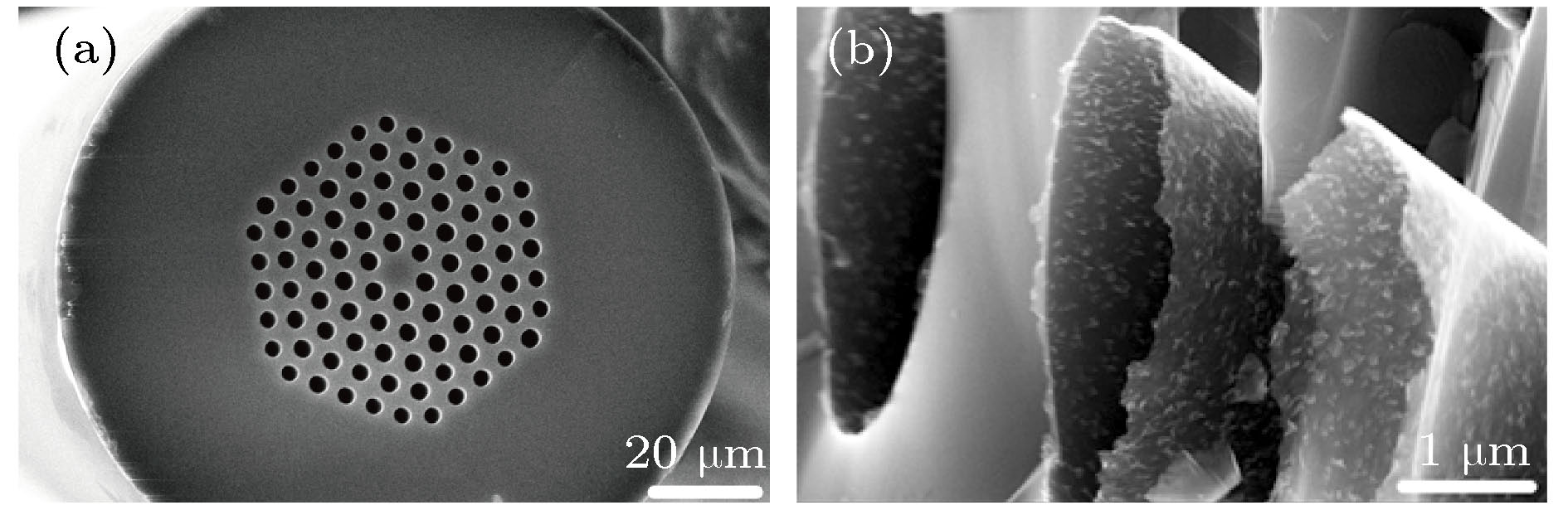 图 2 (a) 用于生长石墨烯的光子晶体光纤端面SEM图; (b) G-PCF破损端面空气孔处突出的管状石墨烯
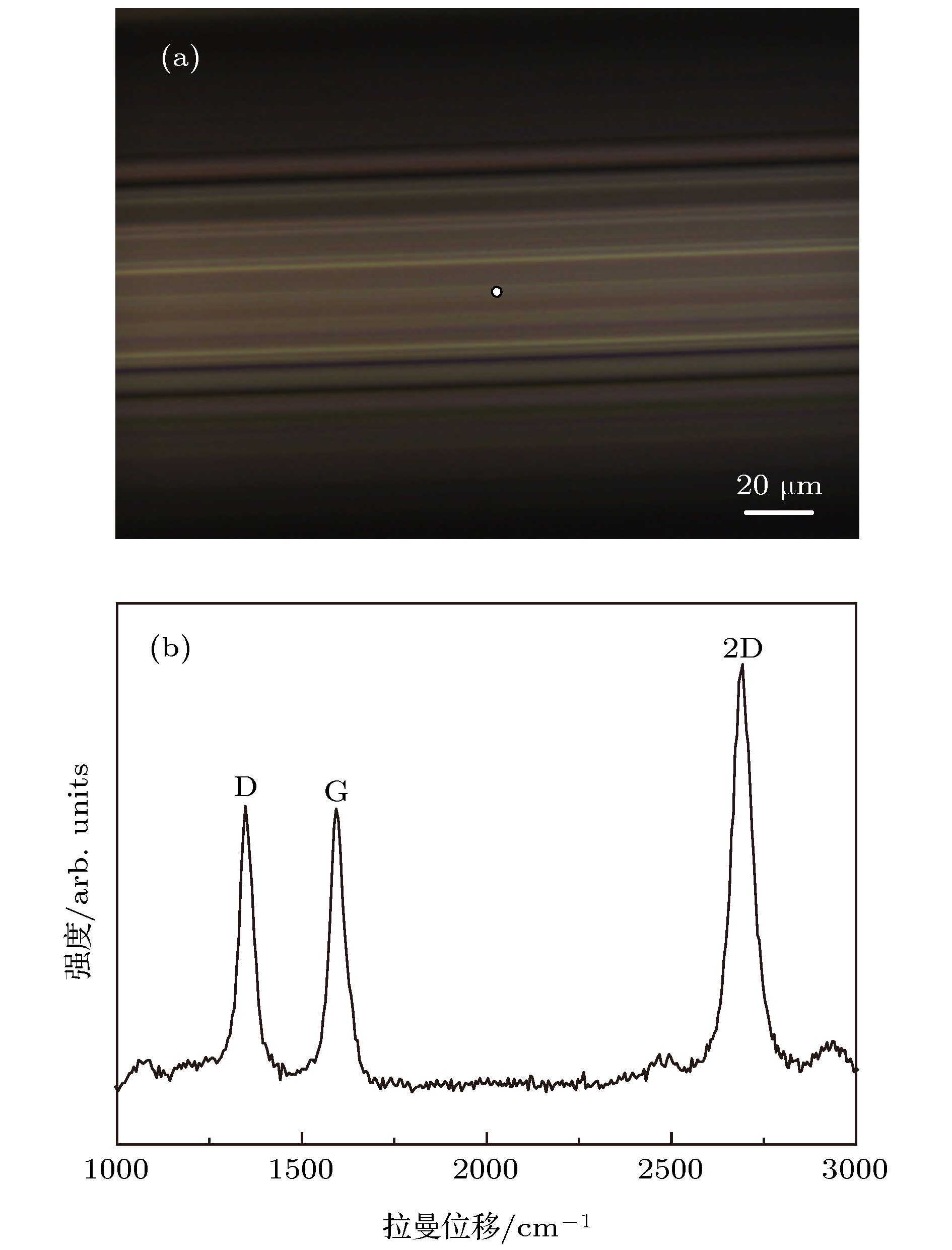 图 3 (a) G-PCF拉曼显微镜成像图; (b) G-PCF拉曼光谱图
 图 4 不同温度下生长的G-PCF拉曼光谱特征参数变化图 (a) G峰半高宽随温度的变化; (b) 2D峰半高宽随温度的变化; (c) I2D/IG随温度的变化; (d) ID/IG随温度的变化
 图 5 不同生长时间下生长的G-PCF拉曼光谱特征参数变化图 (a) G峰半高宽随生长时间的变化; (b) 2D峰半高宽随生长时间的变化; (c) I2D/IG随生长时间的变化; (d) ID/IG随生长时间的变化
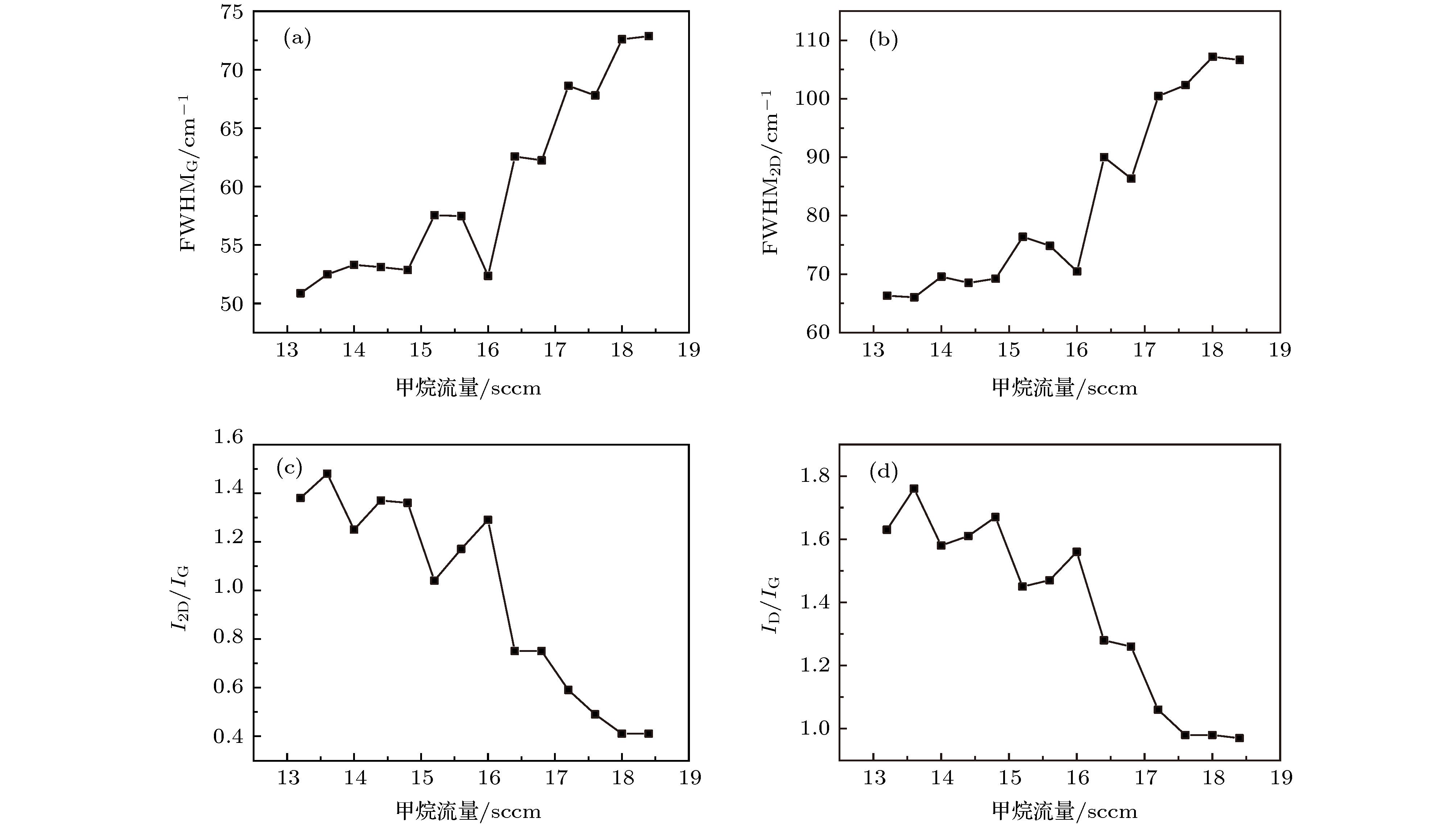 图 6 甲烷流量与G-PCF拉曼光谱的特征参数关系图 (a) G峰半高宽随气体流速的变化; (b) 2D峰半高宽随气体流速的变化; (c) I2 D/IG随气体流速的变化; (d) ID/IG随气体流速的变化
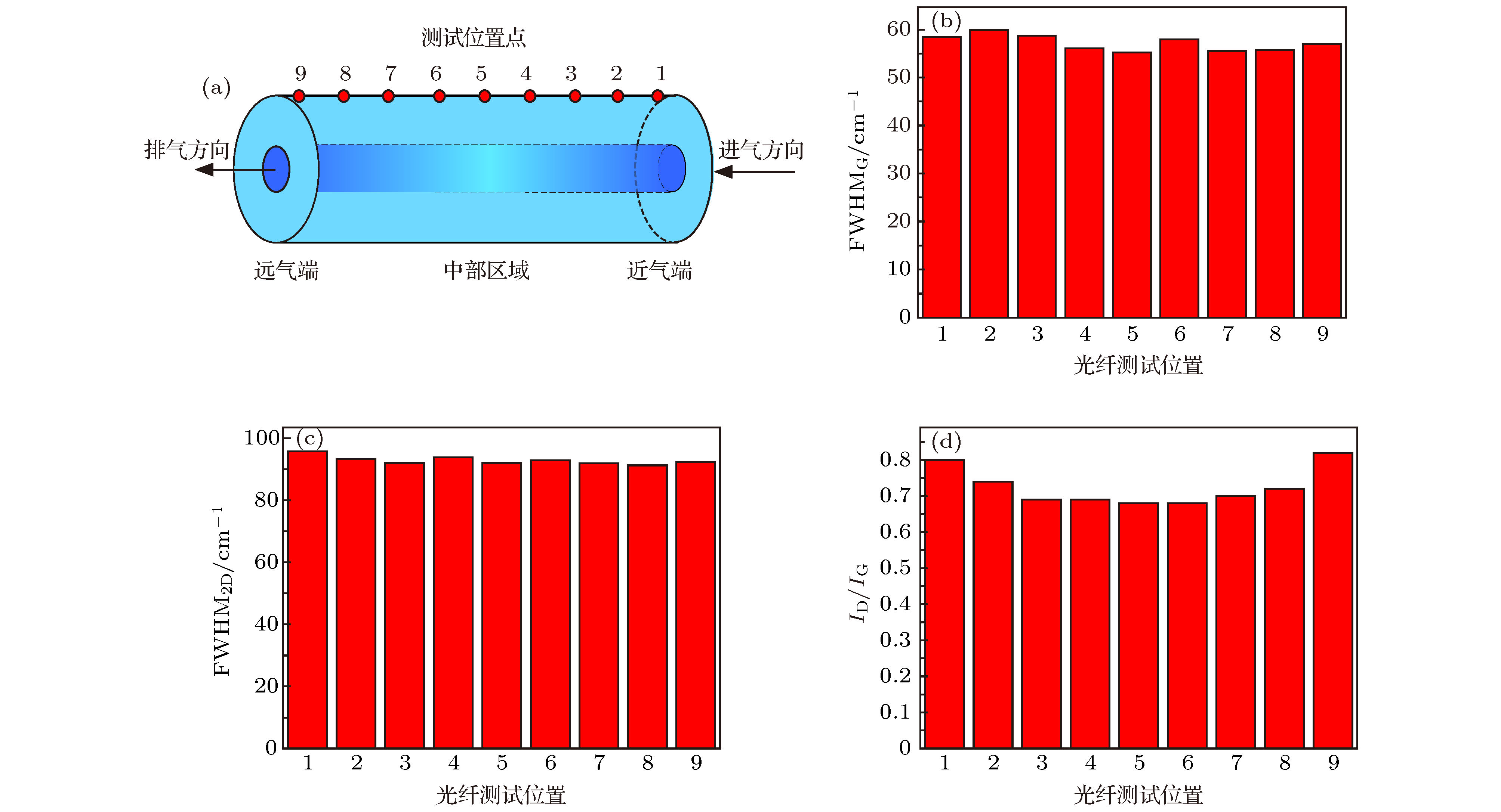 图 7 (a) G-PCF拉曼测试位置示意图; 在9个测试位置上的拉曼光谱特征参数 (b) G峰半高宽, (c) 2D峰半高宽, (d) ID/IG