

全文HTML
--> --> -->室温下, 氢终端金刚石表面2 DHG的浓度范围为1012—1014 cm–2, 霍尔迁移率范围为1—200 cm2/(V·s), 不同晶面的氢终端单晶金刚石在载流子浓度、迁移率、方阻等方面有所不同[5-9]. 根据文献报道, 基于多晶金刚石制备的氢终端场效应晶体管的输出电流往往大于单晶金刚石器件[10-13], 这与多晶金刚石的择优取向是


采用微波等离子体化学气相淀积(MPCVD)的方法在高温高压(HPHT)金刚石衬底上外延生长单晶金刚石, 对其切割分别得到(110)和(111)晶面的单晶金刚石片, 并且基于两种不同晶面的单晶金刚石制备金属-半导体场效应晶体管(MESFET). (110)和(111)晶面单晶金刚石上栅长为6 μm的器件分别获得58.02 mA/mm和80.41 mA/mm的输出电流, 为了研究不同晶面氢终端单晶金刚石的差异性, 我们从材料和器件两个层面进行分析研究.
图1所示为器件的制备流程. 首先使用电子束蒸发的方法在氢终端金刚石表面蒸镀100 nm厚的金[18], 用来与氢终端金刚石形成欧姆接触, 同时保护氢终端表面. 接着进行有源区光刻和金的湿法腐蚀, 使用KI/I2溶液将有源区之外的金腐蚀掉. 再将腐蚀后的样品置于低功率的氧等离子体中处理10 min, 使有源区之外暴露出的氢终端表面变为高阻的氧终端表面, 形成器件之间的隔离区. 接着进行栅窗口光刻, 湿法腐蚀去掉窗口中的金, 光刻胶下方留下的金则作为源、漏电极, 同时由于金的横向腐蚀, 实际的源、漏电极间距大于栅窗口定义出的栅长. 最后再次使用电子束蒸发的方法在样品表面蒸镀100 nm厚的铝, 金属剥离后得到栅电极, 完成整个MESFET器件的制备. 制备的器件栅长为6 μm, 栅宽为50 μm. 对(110)和(111)晶面单晶金刚石片分别进行了原子力显微镜(AFM)、光致发光 (PL)和Raman测试, 用Keithley 4200半导体分析仪测试分析所制成器件的I-V特性、C-V特性.
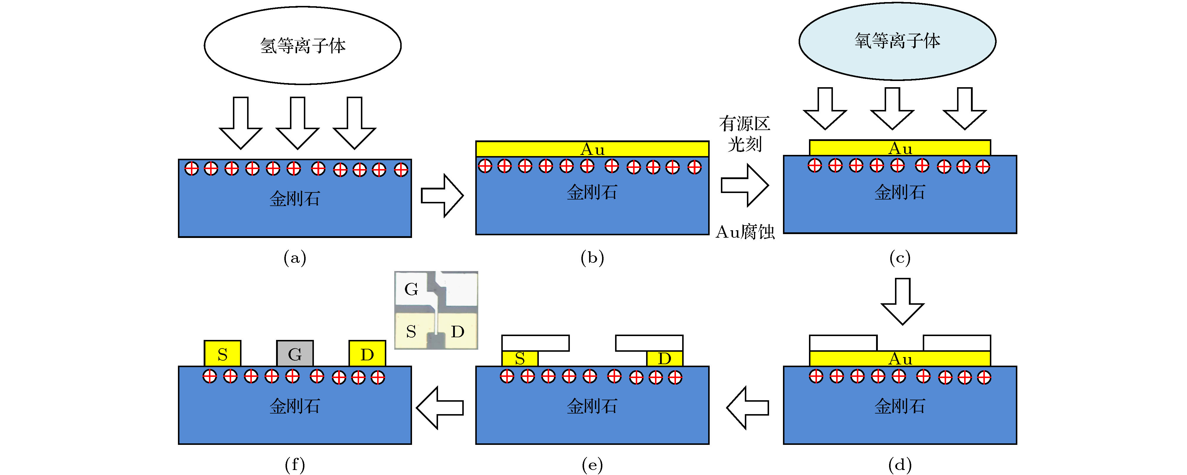 图 1 器件制备流程图 (a)氢等离子体处理; (b) Au沉积; (c)隔离工艺; (d)栅窗口光刻; (e) Au腐蚀; (f) Al沉积及剥离, 右上角为器件俯视图显微照片
Figure1. Schematic diagram of the device fabrication process: (a) Hydrogen plasma treatment; (b) gold deposition; (c) device isolation; (d) gate window photolithography; (e)wet etching of gold; (f) aluminum deposition and lifting off. The inset at the upper right corner of (f) is the top view of the device.
 图 2 氢等离子体处理前的金刚石表面形貌 (a) (110)面; (b) (111)面
Figure2. Surface morphology of the diamond before hydrogen plasma treatment: (a) (110) plane; (b) (111) plane.
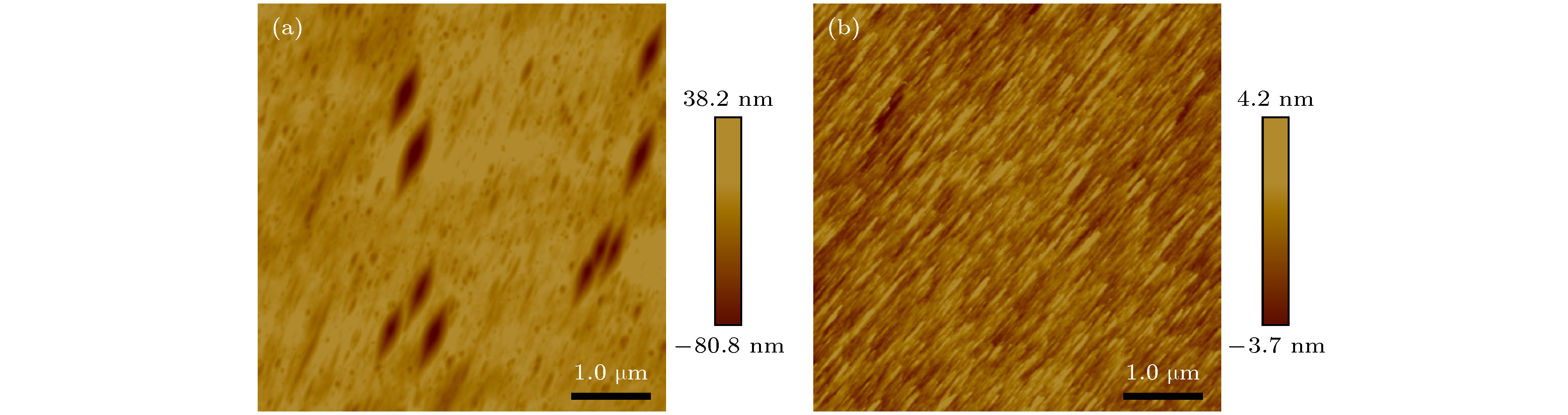 图 3 氢等离子体处理后的金刚石表面形貌 (a) (110)面; (b) (111)面
Figure3. Surface morphology of the diamond after hydrogen plasma treatment: (a) (110) plane; (b) (111) plane.
Raman和PL测试结果如图4所示, 测试时采用的都是波长为514.5 nm的激光器. (110)和(111)面金刚石的拉曼谱都出现了位于1332.5 cm–1的SP3杂化C—C键对应的金刚石特征峰, 峰位没有发生明显的位移, 说明样品中张应力小. 尖锐的特征峰和平整的基线表明(110)和(111)金刚石的结构有序度都很高, 没有明显的非晶相存在. 图4(a)中插图所示为特征峰的半高宽(FWHM), (111)金刚石半高宽为4.0 cm–1, (110)金刚石为3.9 cm–1, 近似一致. 从图4(b)可以看出, (110)和(111)金刚石的PL光谱都有明显的光致发光峰, 尤其在波长约为700 nm附近存在明显的宽峰, 而且该宽峰不是左右对称型的, 这表明其是由多个峰组合而成. 对于CVD金刚石而言, 该发光中心一般与N, Si有关. 此外, PL光谱图中还存在波长为575.7 nm和637.9 nm的发光中心, 且(111)金刚石的峰强度较高, 这表明了两个样品都存在中性的氮空位缺陷(即[N-V]0)、带负电的氮空位缺陷(即[N-V]–)[20,21]. Raman和PL光谱图表明, 源于同一颗CVD单晶金刚石的(110)和(111)金刚石片并没有因为表面晶向不同引起光学性质上的显著差异.
 图 4 不同表面金刚石的 (a) Raman光谱图, (b) PL光谱
Figure4. (a) Raman spectra and (b) photoluminescence (PL) spectra of the diamond plates with different surface orientations.
图5给出制备的栅长LG = 6 μm, 栅宽WG = 50 μm的MESFET的栅-源二极管的I-V特性. VGS = 3 V时, 器件A与B的反向栅漏电皆小于2 × 10⁻⁶ A/cm2. 然而当栅电压小于–3 V时, 器件A与B的正向栅漏电迅速增大, 并且在栅电压为–4 V时分别达4.0 × 10⁻⁴ 和1.4 × 10⁻⁴ A/cm2. 器件A栅泄漏电流较大的可能原因之一是氢等离子体处理后(110)氢终端金刚石表面出现了刻蚀坑. 本文的器件和大量采用Al栅的氢终端金刚石MESFET的栅正向耐压都远大于Al与氢终端金刚石表面的肖特基势垒高度(0.62 eV)[22], 其原因可能是在Al与氢终端金刚石之间生成一层氧化铝, 这一氧化层使Al栅的氢终端金刚石MESFET器件实际上成为了金属-氧化物-半导体(MOS)的器件结构[23-25]. 而且, 器件A和B的栅漏电近似与3 nm Al2O3(由铝膜氧化得到)MOS器件[26]处于同一水准, 但是高于34.1 nm HfO2 (4 nm ALD-HfO2/30.1 nm SD-HfO2) MOS器件[27], 这也从另一面说明Al栅MESFET器件中应存在非故意引入的氧化铝介质层. 当栅电压小于–3.3 V时, 栅-源二极管的I-V特性可以通过关系式

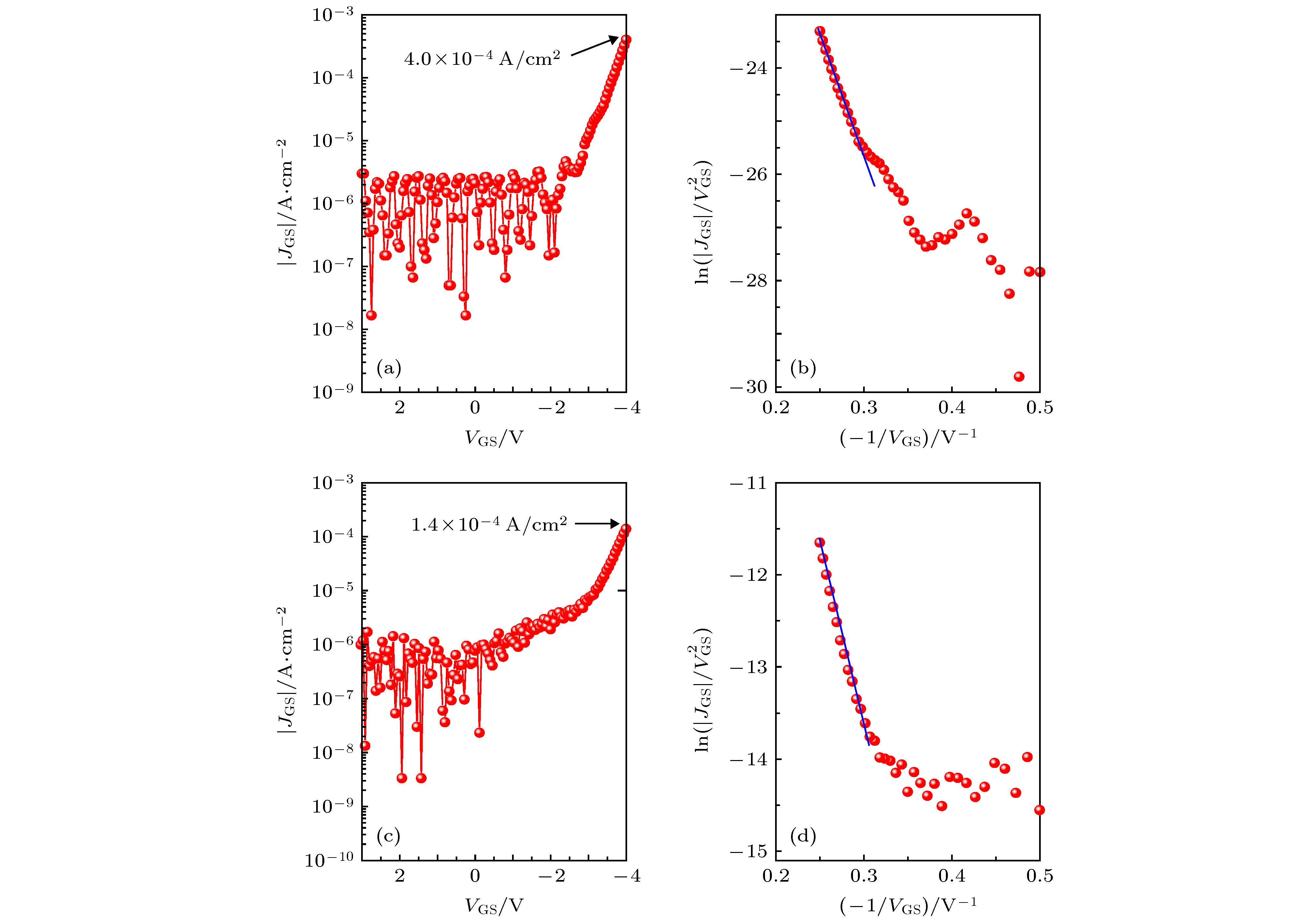 图 5 栅-源二极管的I-V特性以及正向偏置下的拟合结果 (a) A器件I-V特性; (b) 图(a)部分栅压区的拟合结果; (c) B器件I-V特性; (d) 图(c)部分栅压区的拟合结果
Figure5. Current-voltage characteristics of the gate-source diodes and fitting results at the forward bias: (a) and (b) are for device A; (c) and (d) are for device B.
器件的输出特性如图6所示, 都是耗尽型的p沟道器件. 器件A的最大输出电流IDmax在栅电压VGS = –4 V时为–58.02 mA/mm, 而器件B的为–80.41 mA/mm, 约为器件A的1.4倍. 线性区的导通电阻Ron随着栅电压变化而变化, 当VGS = –4 V时, 器件A的导通电阻Ron为71.93 Ω·mm, 器件B的为48.51 Ω·mm, 后者只有前者的67%. 器件转移特性如图7所示, 两者都是VDS = –6 V时测得的. 从

 图 6 输出特性 (a)器件A; (b)器件B
Figure6. Output characteristics: (a) Device A; (b) device B.
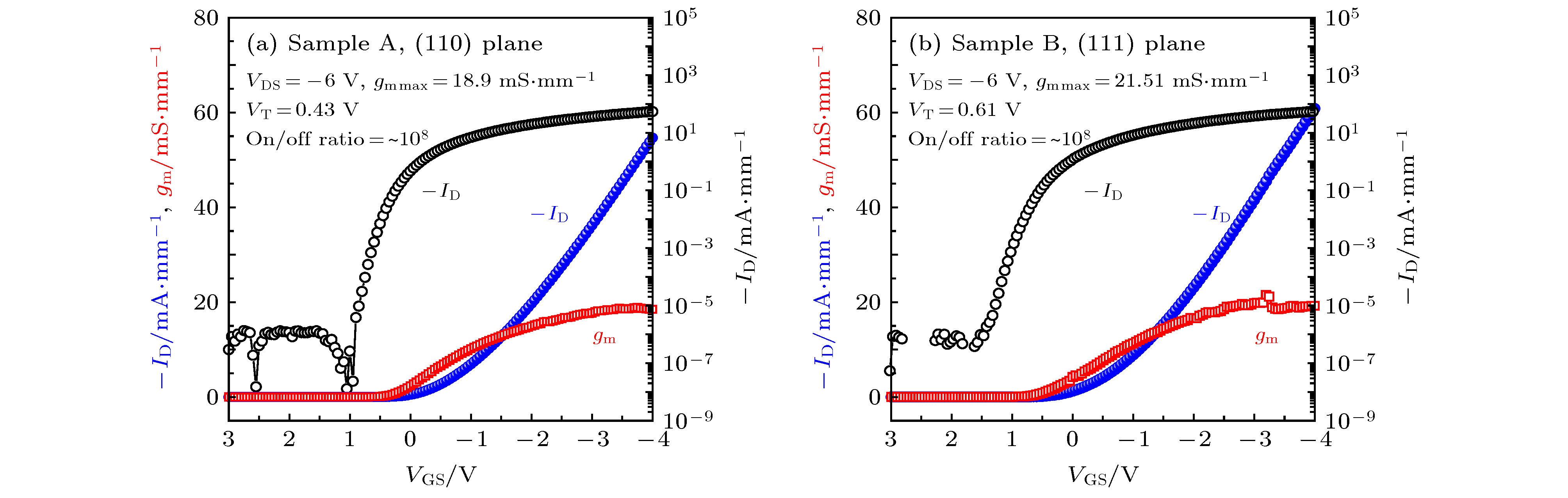 图 7 转移特性 (a)器件A; (b)器件B
Figure7. Transfer and transconductance characteristics: (a) Device A; (b) device B.
图8总结了部分已报道的栅长4—11 μm的单晶金刚石场效应管最大饱和电流和最大跨导值随栅长的变化关系, 同时列入本文的器件数据. 可以发现, 在长沟道器件中, 栅长6 μm的器件获得的最大饱和电流和跨导都拥有明显的优势, 尤其是(111)金刚石上的器件B.
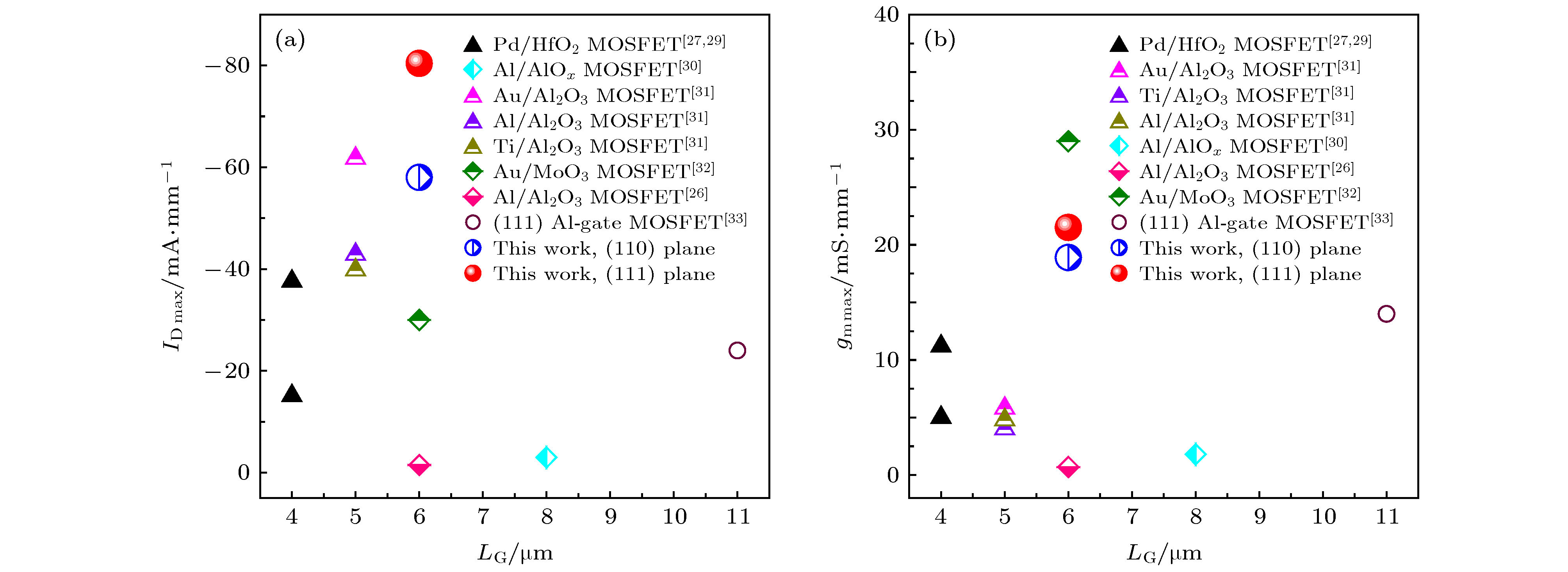 图 8 氢终端金刚石场效应管输出电流(a)和最大跨导(b)随栅长的变化(数据来自文献[26,27,29—33]), MOSFET器件给出了栅金属和栅介质
Figure8. Summary of the reported (a) IDmax and (b) maximum transconductance of hydrogen-terminated diamond FETs dependent on the gate length[26,27,29-33]. The gate metal and gate dielectric are given for MOSFETs.
场效应管器件的特性主要由栅下沟道中载流子浓度、分布以及输运特性来决定的. 为了深入分析器件的特性, 测试了器件在1 MHz下栅-源二极管的C-V曲线, 结果如图9所示. 设栅下沟道中载流子的浓度为pch, 通过C-V曲线以及关系式

 图 9 栅源二极管的C-V特性以及计算出的沟道载流子浓度随VGS的变化 (a)器件A; (b)器件B
Figure9. Capacitance-voltage characteristics of the gate-source diode and the calculated hole density in the gated channel as a function of VGS: (a) Device A; (b) device B.
由于器件A和B的沟道载流子浓度差异并不大, 而饱和电流和导通电阻的差异较大, 可以推测出(111)面的沟道载流子迁移率应略高于(110)面的沟道载流子迁移率, 方阻则应低于(110)面. Kawarada等[9]报道了氢终端金刚石的霍尔特性, Kasu 等[34]报道了吸附 NO2 的氢终端金刚石的霍尔特性, 都展示了(111)面的方阻低于(110)面, 且两者的方阻都明显低于(100)面, 有利于制备高性能器件. 本文的结果从器件层面有力地证明了这一结论.
基于(110)和(111)单晶金刚石制备了栅长为6 μm的Al栅氢终端金刚石MESFET器件A与B. 在VGS = –4 V时, 器件A的导通电阻为71.93 Ω·mm, 获得–58.02 mA/mm的最大饱和电流; 而器件B的导通电阻为48.51 Ω·mm, 大小只有器件A的67%, 最大饱和电流为–80.41 mA/mm, 约为器件A的1.4倍. 由转移特性可得, 器件A与B的最大跨导分别为18.9和21.51 mS/mm, 且都有较大的开关比约108. 通过C-V曲线我们得到器件A的栅下沟道中最大载流子浓度为1.34 × 1013 cm–2, 器件B的为1.45 × 1013 cm–2, 近似是器件A的1.08倍. 器件B拥有大饱和电流和低导通电阻的主要原因是其方阻更低. 本文的器件数据和已报道的栅长4—11 μm的单晶金刚石场效应管进行了比较, 可以发现, 最大饱和电流和跨导都拥有明显的优势, 尤其是(111)金刚石制备的氢终端场效应管.
