Fund Project:Project supported by the Jiangsu Specially-Appointed Professor and the Science Research Funds for Nanjing University of Posts and Telecommunications, China (Grant Nos. SZDG20180007, NY217116, KFJJ20170101, NY219014, NY218110), the China Postdoctoral Science Foundation (Grant No. 2018M642290), the National Natural Science Foundation of China (Grant No. 61804079), the University Natural Science Foundation of Jiangsu Province, China (Grant No.18KJD510005), the Innovative Doctor Program, China (Grant Nos. CZ1060619001), and the Graduate Research and Innovation Projects of Jiangsu Province, China (Grant Nos. SJCX19_0256, SJKY19_0811, SJKY19_0806)
Received Date:04 July 2019
Accepted Date:27 August 2019
Available Online:26 November 2019
Published Online:05 December 2019
Abstract: Inspired by the working mechanism of human brain, the artificial neural network attracts great interest for its capability of parallel processing, which is favored by big data task. However, the electronic synapse based on CMOS neural network needs at least ten transistors to realize one biological synaptic function. So, CMOS-based neural network exhibits obvious weakness in speed, power consumption, circuit area and resource utilization and so on, compared with biological synapses. Therefore, how to build neuromorphic circuits and realize biological functions by constructing electronic synapses with low power consumption and high integration density have become the key points for human to realize brain-like computing system. Memristors, as the fourth basic component, is a two-terminal nonlinear device possessing nonlinear conductance that can be tuned continuously. For that special characteristic, it is very similar to biological synapse whose connection strength can be adjusted continuously. In this article, first of all, we study the electrical characteristic of the Cu/MXene/SiO2/W memristor. When applying a positive DC sweeping voltage to the Cu electrode, the Cu electrode is oxidized, generating Cu2+. The generated Cu2+ in function layer tends tomove towards the bottom electrode under the action of electric field. Near the bottom electrode the Cu2+ moving from top electrode are reduced, generating a conductive Cu atom. With Cu atoms accumulating and extending from bottom electrode to top electrode, the memristor is gradually converted from the initial high resistance state (HRS) into the low resistance state (LRS). Secondly, combining with HP model of memristor, we utilize Verilog A language to simulate memristor in the experiment we conducted. Subsequently, we successfully construct the artificial synaptic unit and design the weight differential circuit with self-feedback branch. In the above circuit, we successfully implementa classical " Pavlov's dog” experiment. By applying the sinusoidal signal and pulse signal to the synaptic unit for testing and training it, respectively, the circuit realizes the convention between the conditions that unconditioned stimulus producing unconditioned response to conditioned stimulus producing conditions response. This work takes memristor as a center, through modelling the electrical characteristic of Cu/MXene/ SiO2/W device, we construct a neuromorphic circuit with weight differential branch andself-feedback branch, successfully simulate the classical learning behavior of biological synapses, and realizes the whole process of biologically conditioned reflex, which is illustrated in detail in the experiment on " Pavlov′s dog”. The results will provide effective guidance forconstructing a large scale and high density neuromorphic circuitbased on memristor, thus promoting the realization of brain-like computation in the future. Keywords:memristor/ artificial synapse/ conditioned reflex/ neuromorphiccircuits
全文HTML
--> --> --> 1.引 言随着冯·诺依曼瓶颈渐显, 传统计算机将无法满足大数据时代信息处理的需求, 而与之相对的类脑计算受到研究人员越来越多的关注[1,2]. 人脑内部具有1011数量级的神经元, 通过之间103—104倍数量的突触连接构成了一个复杂的神经网络[3-5]. 不同于现今的电子计算机, 人脑可以基于海量的神经元和突触以并行、分布式的方式处理信息, 其中突触连接强度的改变, 被认为是人脑学习和记忆的基础[6-8]. 受大脑的启发, 人工神经网络的出现在一定程度上成功实现了大量数据的并行处理[9,10]. 其中在硬件实现方面, 基于互补金属氧化物半导体的电子突触构建的人工神经网络至少需要10个晶体管才能实现一个生物突触的功能, 因此进行任务处理时, 和生物神经系统相比, 在速度、能耗、电路面积以及资源利用率等方面存在着明显的弱点[11-13]. 因此, 构建低功耗、高集成度的电子突触, 搭建神经形态系统成为实现类脑智能的关键. 忆阻器是一种具有模拟渐变式记忆功能的双端非线性器件[14,15]. 其阻态的变化受到内部金属离子或氧空位迁移的调控, 其调节机制与突触权重受神经递质刺激后产生的调节过程极为类似[16-18]. 正是由于这种物理机理上的相似性以及器件的易于集成、低功耗、尺寸小等特性, 忆阻器成为构建人工突触的极佳选择[19,20]. 然而目前的研究大多数集中在利用不同结构和材料的器件产生忆阻行为以模拟生物突触可塑性的阶段[21,22], 对于如何利用忆阻器实现神经形态系统级的功能尚缺少研究报道. 本文为实现电路对刺激信号的及时响应, 选择二维材料MXene作为忆阻器插入层. 与其他二维材料相比, MXene具有优异的机械性能、较大的比表面积[23,24], 基于MXene的忆阻器能在更短时长的训练信号下改变忆阻器导态[25-27]. 首先, 研究了Cu/MXene/SiO2/W忆阻器的电学特性; 然后, 基于该器件的电学特性, 以分段线性窗函数结合惠普的氧化物忆阻器模型[28], 使用Verilog A语言对该忆阻器进行建模; 随后, 基于该器件模型构建了人工突触单元并设计了权值差分电路. 在电路工作过程中, 分别采用正弦电压信号以及脉冲电压信号对突触权值进行测试和反馈训练, 最后实现了经典条件反射行为[29]. 这一工作对未来构造以忆阻器为基础单元的大规模神经形态电路和智能运算系统, 具有十分重要的意义. 2.器件介绍如图1(a)所示, 双端Cu/MXene/SiO2/W忆阻器以厚度100 nm的活性金属Cu、90 nm的金属W分别作为顶电极和底电极. 在两个电极之间, 以旋涂法制备的二维材料MXene以及磁控溅射制备的SiO2为阻变层[30]. 器件上表面在金相显微镜下如图1(b)所示, 可以清晰地看到顶部的金属电极(直径约150 μm). MXene材料以团簇状堆积, 在原子间电势作用下在团簇状结构内部产生强电场. 图1(c)为二维材料MXene的扫描电镜图像, 可以清晰地看到MXene的二维层状结构. MXene的二维层状结构总体呈团簇状, 具有极小曲率, 在电极电压作用下能产生较大电场. 在施加电压时可以在一定程度引导导电细丝的生长, 提高导电通道产生的规律性, 进而有望提高忆阻器的电学特性的稳定性. 图1(d)为该器件的工作机理示意图. 当对Cu电极施加正电压, W电极接地时, 顶电极的Cu发生氧化反应生成Cu2+, Cu2+在定向电场作用下通过阻变层到达底电极, 并且在底电极与附近的电子结合还原生成Cu原子, 随着底电极附近Cu原子聚集并向顶电极延伸, 忆阻器逐渐由初始高阻态(high resistance state, HRS)转变到低阻态(low resistance state, LRS). 忆阻器的电阻状态受到内部Cu2+在电场作用下的定向移动而被连续调节[31], 这与图1(e)中生物突触连接强度在神经递质移动的影响下发生的权重改变极为相似. 图 1 (a) Cu/MXene/SiO2/W忆阻器结构及电学测试示意图; (b)二维材料MXene的扫描电镜图; (b) 金相显微镜下忆阻器表面结构; (d)正向偏压下器件工作机理示意图; (e)受到刺激信号, 突触前膜、突触后膜之间神经递质迁移示意图 Figure1. (a) The device structure and measurement of Cu/MXene/SiO2/W memristor; (b) surface structure of memristor under metallographic microscope; (c) the scanning electron microscope result of two-dimensional material MXene; (d) the physical mechanism of the Cu/MXene/SiO2/W memristor under positive voltagestimulus; (e) the neurotransmitter transfer between pre- and postsynaptic membrane after stimulus.
3.测试与仿真结果经典条件反射又称巴普洛夫反射, 其中最著名的实验为巴普洛夫的狗的唾液条件反射. 实验第一阶段, 狗看到食物本能的发生流涎反应, 属于无条件反射行为, 此时食物为非条件刺激(unconditional stimulus, US), 流涎的行为为非条件反应(unconditional reaction, UR); 实验第二阶段, 当没有经过训练, 单独出现铃声时, 狗并不会流涎, 此时铃声为中性刺激(neural stimulus, NS); 实验第三阶段, 在发出铃声的同时提供食物训练, 狗出现流涎反应; 实验第四阶段, 单独发出铃声, 狗经过第三阶段的训练学习后出现流涎反应, 此时流涎属于条件反应(conditional reaction, CR), 铃声由NS转变为条件刺激(conditional stimulus, CS). 为了构造基于忆阻器的神经形态电路, 实现经典条件反射. 首先我们用惠普模型对实验中忆阻器伏安特性进行了拟合, 使用硬件描述语言Verilog A针对忆阻器电学特性对本文中新型二维材料忆阻器进行建模[32,33]. 图2(a)所示为惠普研究团队提出的忆阻器线性漂移模型, 该模型虽能较好地复现忆阻器的连续导态特性, 但在纳米尺度下, 小电压产生的大电场将会进一步在界面附近产生空位的非线性漂移[34], 无法再使用线性漂移模型. 因此, 我们通过增加以下形式的分段线性窗函数$f(x)$解决该边界问题[35]: 图 2 (a)惠普研究小组提出的忆阻器模型; (b)忆阻器模型仿真数据与实验测试数据拟合 Figure2. (a) Memristor model reported by HP group; (b) the fitting of experimental data and the simulation data.
即发生“流涎”事件. 到此实现条件反射全部过程. 图4(a)为实现条件反射时, 输入输出信号的波形变化. 波形包含学习前、学习过程、学习后三个阶段. 学习前: “肉”事件信号输入时, 对应上述分析过程的${U_{{\rm{o1}}}} > 0$, 输出信号与输入信号同相, 判断为“流涎”; “铃声”事件信号输入时, 对应上述分析过程的${U_{{\rm{o}}2}} < 0$, 输出与输入信号反相, 判断为未发生“流涎”, 此时“铃声”为中性刺激. 学习过程: “铃声”、“肉”事件信号同时输入, 输出信号为两支路单独工作时输出信号的叠加, 对应上述分析过程的${U_{{\rm{o}}3}} > 0$. 此时满足条件“铃声”、“肉”事件同时发生, 触发训练模块输出训练信号, 由于电压脉冲能够对忆阻器Ma产生连续调节作用[37-39], 该电路中以方波脉冲作为训练信号作用于铃铛支路, 如该过程中Vout所示. 当满足条件${R_{{{\rm{M}}_{\rm{a}}}}} < {R_{\rm{a}}}$时, 对应上述分析过程的${U_{{\rm{o4}}}} > 0$, 满足当输入只有“铃声”信号时, 输出波形呈现出由负相${U_{{\rm{o}}2}} < 0$到正相${U_{{\rm{o4}}}} > 0$的变化过程, 该变化说明学习过程结束, “铃声”转变为条件刺激. 图 4 (a)仿真过程施加的信号以及各自对应的结果图; (b)对电路中忆阻器模型进行直流电压扫描, 流经忆阻器的电流随仿真时间的变化; (c)训练过程中, 流经忆阻器Ma的电流随时间的变化 Figure4. (a) The signals inputted into the circuit and corresponding output waveform, respectively; (b) the change of current flowing through the memristor against timeduring DC voltage sweeping; (c) the change of current through the memristor Ma during training process.
 图 1 (a) Cu/MXene/SiO2/W忆阻器结构及电学测试示意图; (b)二维材料MXene的扫描电镜图; (b) 金相显微镜下忆阻器表面结构; (d)正向偏压下器件工作机理示意图; (e)受到刺激信号, 突触前膜、突触后膜之间神经递质迁移示意图
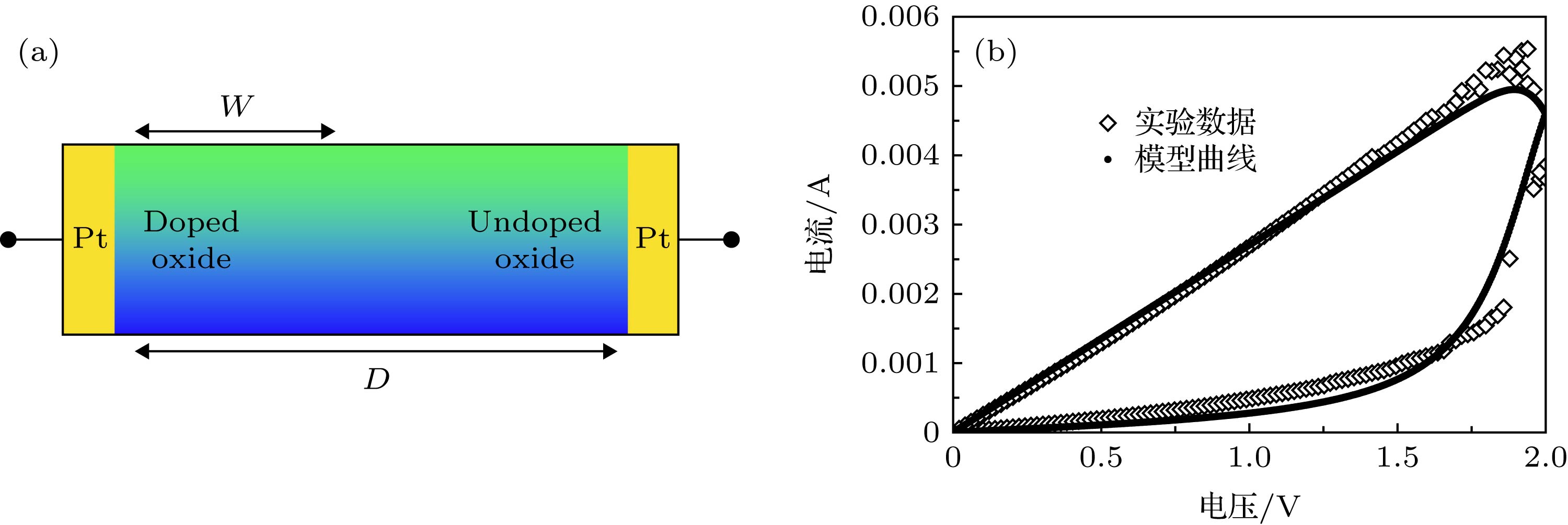 图 2 (a)惠普研究小组提出的忆阻器模型; (b)忆阻器模型仿真数据与实验测试数据拟合
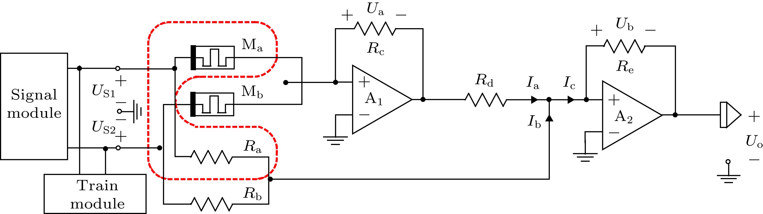 图 3 实现条件反射的神经形态电路


 图 4 (a)仿真过程施加的信号以及各自对应的结果图; (b)对电路中忆阻器模型进行直流电压扫描, 流经忆阻器的电流随仿真时间的变化; (c)训练过程中, 流经忆阻器Ma的电流随时间的变化