全文HTML
--> --> -->目前, Ti基多层金属结构(Ti/Al/Ni/Au)是应用于n型GaN欧姆接触最为广泛的电极材料,如图1所示. 通常是在n型GaN表面沉积多层金属结构, 其后是快速热退火(RTA)工艺, 在高于800 ℃的温度下快速退火, 使金属间、金属-半导体间发生固相反应以获得低的接触电阻[8—15]. van Daele等[16]发现, 若仅用单层的Ti作为电极形成欧姆接触, 退火后的金属-半导体界面处会形成大的空隙. 这是由于金属Ti在退火过程中会夺取GaN中的N发生固相反应产生TiN以及Ga-Ti合金, 导致了接触界面处的GaN分解. 这种反应在较高的温度下退火时, 发生得更加彻底, 导致了更大的空隙出现. Al的引入可以一定程度地抑制GaN的分解, 减少金属-半导体界面处的“空洞”产生. 然而传统的Ti金属电极需要的退火温度都在800 ℃以上[11], 作为Ti基欧姆接触电极体系中的关键金属Al, 其熔点为660.4 ℃[17]. Gong等[18]发现电极材料在退火的过程中, Al处于熔融状态, 部分Al会外溢与Au形成晶体颗粒状合金, 使电极表面变得粗糙. 这种粗糙的电极表面会导致尖端放电现象, 使功率电子器件的击穿特性下降. 对于微波器件, 会引起电流分布不均匀以及信号衰减. GaN器件在大电流环境下工作时, 还可能导致电极表面凸起开裂, 从而影响器件的可靠性. 因此, 寻找合理的欧姆电极金属体系以及开发欧姆电极低温退火工艺可以提高电极的性能.
 图 1 目前最常应用于n型GaN欧姆接触的Ti基多层金属体系
Figure1. Ti-based multilayer metal system most commonly used in n-type GaN ohmic contact
近些年来, 很多课题组就电极金属材料的选择、退火工艺等问题对n型GaN欧姆接触进行了研究[19]. France等[20]使用V/Al/V/Au (15/18/20/200 nm)金属体系, 在N2氛围中650 ℃退火30 s, 得到的比接触电阻率为2.2×10⁻⁶ Ω·cm2. Park等[21]在GaN半极性面上使用Ti/Ta/Al/Au (10/10/150/30 nm)作为电极, 在N2氛围中600 ℃条件下退火1 min, 得到了比接触电阻率为4.8×10⁻⁵ Ω·cm2. 2017年, Zhao等[22]在没有退火的条件下, 制作了比接触电阻率为3×10⁻⁴ Ω·cm2的Al/Au (30/300 nm)电极.
理论上, 功函数接近GaN电子亲和势的金属都能与n型GaN形成良好的欧姆接触[23], 因此与Ti处于同一族且功函数较低的Hf[24]是与n型GaN形成欧姆接触的更好选择,如表1所示. 本文制备了n型GaN基Hf/Al欧姆电极, 研究了不同退火条件对其欧姆接触性能和结构特性的影响, 并与Ti/Al电极进行了对比.
| 金属 | 功函数/eV[24] | 熔点/K[17] | 电阻率/Ω·cm2 (273 K)[25] |
| Ti | 4.33 | 1943 | 4.2×10⁻⁶ |
| Al | 4.24 | 933.60 | 2.4×10⁻⁶ |
| Ni | 5.35 | 1728 | 6.24×10⁻⁶ |
| Au | 5.31 | 1337.58 | 2.03×10⁻⁶ |
| Zr | 4.05 | 2128 | 3.86×10⁻⁶ |
| Hf | 3.94 | 2504 | 3.27×10⁻⁶ |
表1不同金属的功函数、熔点、电阻率 (273 K)
Table1.Work function, melting point and resi-stivity of different metals.
在本文中, 测量电极欧姆接触比接触电阻率使用的是圆点型传输线模型(dot CTLM), 具体结构如图2所示. 它是由8个半径为60 μm的内圆和不同半径的外圆所组成, 外圆半径与内圆半径的差值分别为5, 10, 15, 20, 25, 30, 35, 40 μm.
 图 2 实验中用到的圆点型传输线模型(dot CTLM)结构
Figure2. The scheme of dot circular transmission line model (dot CTLM) in this experiment
欧姆接触的样品处理过程如下.
1) 划片: 将大小为4英寸的n型GaN原片进行激光划片, 切割成为多片尺寸为1.5 cm×1.5 cm的正方形小片.
2) 表面清洗: 样品先分别在丙酮, 无水乙醇, 去离子水中各超声清洗15 min以去除有机物与表面颗粒. 随后使用两步法清洗样品, 将样品置于SC1溶液(NH4OH∶H2O2∶H2O = 1∶1∶5)中煮沸10 min以去除表面氧化物, 置于SC2溶液(HCl∶H2O2∶H2O = 1∶1∶5)中煮沸10 min以去除碱性物质以及过渡族金属. 样品取出后用去离子水冲洗3 min, 最后将样品分别在丙酮、无水乙醇、去离子水中超声清洗各15 min, 氮气吹干.
3) 光刻: 制备好光刻掩膜版, 按照UV光刻法工艺标准流程进行操作. 涂胶→前烘→光刻→显影→底膜处理. 在本文的实验中, 使用的光刻胶为负胶.
4) 电极的制备: 将样品送至磁控溅射反应室中, 通过磁控溅射工艺依次溅射Hf/Al (30/300 nm)、Ti/Al (30/300 nm)的金属电极薄膜.
5) 剥离: 使用丙酮超声清洗蒸镀有电极的样品, 并随时使用显微镜进行观测, 超声至附有光刻胶的区域完全剥离为止. 之后将样品分别置于无水乙醇、去离子水中各超声清洗15 min, 氮气吹干.
6) 快速热退火: 将所有样品分为三组, 确保每一组都有不同体系的电极. 分别在650 ℃, N2氛围下退火60 s以及在850 ℃, N2氛围下退火30 s, 另一组样品不进行退火处理.
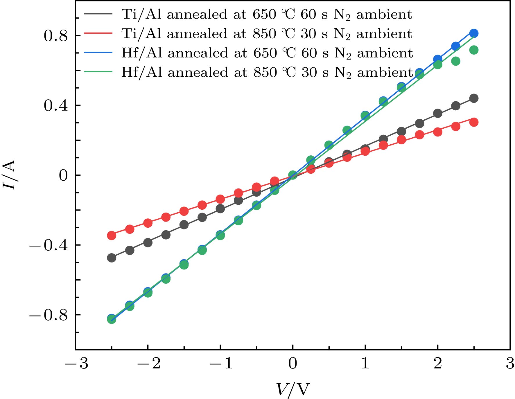 图 3 不同退火条件下Ti/Al, Hf/Al样品间距为10 μm的电极之间的I-V曲线
Figure3. I-V curve between Ti/Al, Hf/Al pads with 10 μm spacing anneales at different condition.
从图3可以看出, 所有样品的I-V曲线均表现出了欧姆接触特性. 其中, 在N2氛围中进行650 ℃退火60 s的Hf/Al电极样品具有最低的电阻.
根据dot CTLM模型测试原理, 测量计算出了各种材料电极在不同退火条件下的比接触电阻率, 列于表2.
| 样品名称 | 退火条件 (N2) | 比接触电阻率/Ω·cm2 |
| Hf/Al | no annealing | 1.21×10⁻⁴ |
| Hf/Al | 650 ℃ 60 s | 4.28×10⁻⁵ |
| Hf/Al | 850 ℃ 30 s | 1.13×10⁻⁴ |
| Ti/Al | 650 ℃ 60 s | 5.85×10⁻⁵ |
| Ti/Al | 850 ℃ 30 s | 1.27×10⁻⁴ |
表2各电极样品在不同退火条件下的比接触电阻率
Table2.Specific contact resistivity of each electrode sample at different annealing conditions.
由表2 Ti/Al, Hf/Al电极样品在不同退火条件下的比接触电阻率可知: Hf/Al电极在没有退火的情况下比接触电阻率为1.21×10–4 Ω·cm2, 在650 ℃的退火条件下比接触电阻率为4.28× 10⁻⁵ Ω·cm2, 在850 ℃的退火条件下比接触电阻率为1.13×10⁻⁴ Ω·cm2; Hf/Al电极在低温退火(650 ℃)条件下具有更好的欧姆接触性能; 而Ti金属电极, Ti/Al电极样品在650 ℃的退火条件下比接触电阻率为5.85×10⁻⁵ Ω·cm2, 当退火温度为850 ℃时, 比接触电阻率为1.27×10⁻⁴ Ω·cm2. 在相同的退火温度下, Hf/Al比Ti/Al有更低的比接触电阻率.
对650 ℃退火条件下的Hf/Al样品进行了深度剖析的AES测试. 图4显示了在650 ℃条件下退火前后Hf/Al电极与n型GaN材料中各种元素的深度分布情况. 可以观察到, 在650 ℃条件下退火60 s后, 两种金属材料已经混合到了一起, 并扩散到了GaN材料当中.
 图 4 Hf/Al电极样品深度剖析的AES图 (a)未退火; (b) 650 ℃退火60 s
Figure4. AES depth profiles of Hf/Al electrodes: (a) No annealing and (b) after annealing at 650 ℃ for 60 s in N2 ambient.
这意味着在金属电极与GaN材料之间的接触界面出现了掺杂层, 这类似于Ti基金属电极与n型GaN形成欧姆接触的原因[26]. N原子在退火过程中扩散到金属层中与Hf-Al合金反应生成氮化物, 这导致了GaN表面留下了N空位, 这些N空位成了GaN的n型施主原子, 相当于n型掺杂. 这有助于形成电阻率较低的欧姆接触.
图5展示了不同退火条件下的Ti/Al, Hf/Al电极截面SEM图像. 可以发现, 正如文献记载[12], Ti/Al电极在650 ℃退火条件下的金属-半导体界面处出现了“空洞”的现象, 这种现象在850 ℃的退火条件下更为明显. 而Hf/Al电极在不同退火条件下的界面处都没有出现这样的情况. 这种空隙的出现, 也是导致比接触电阻率变大的原因.
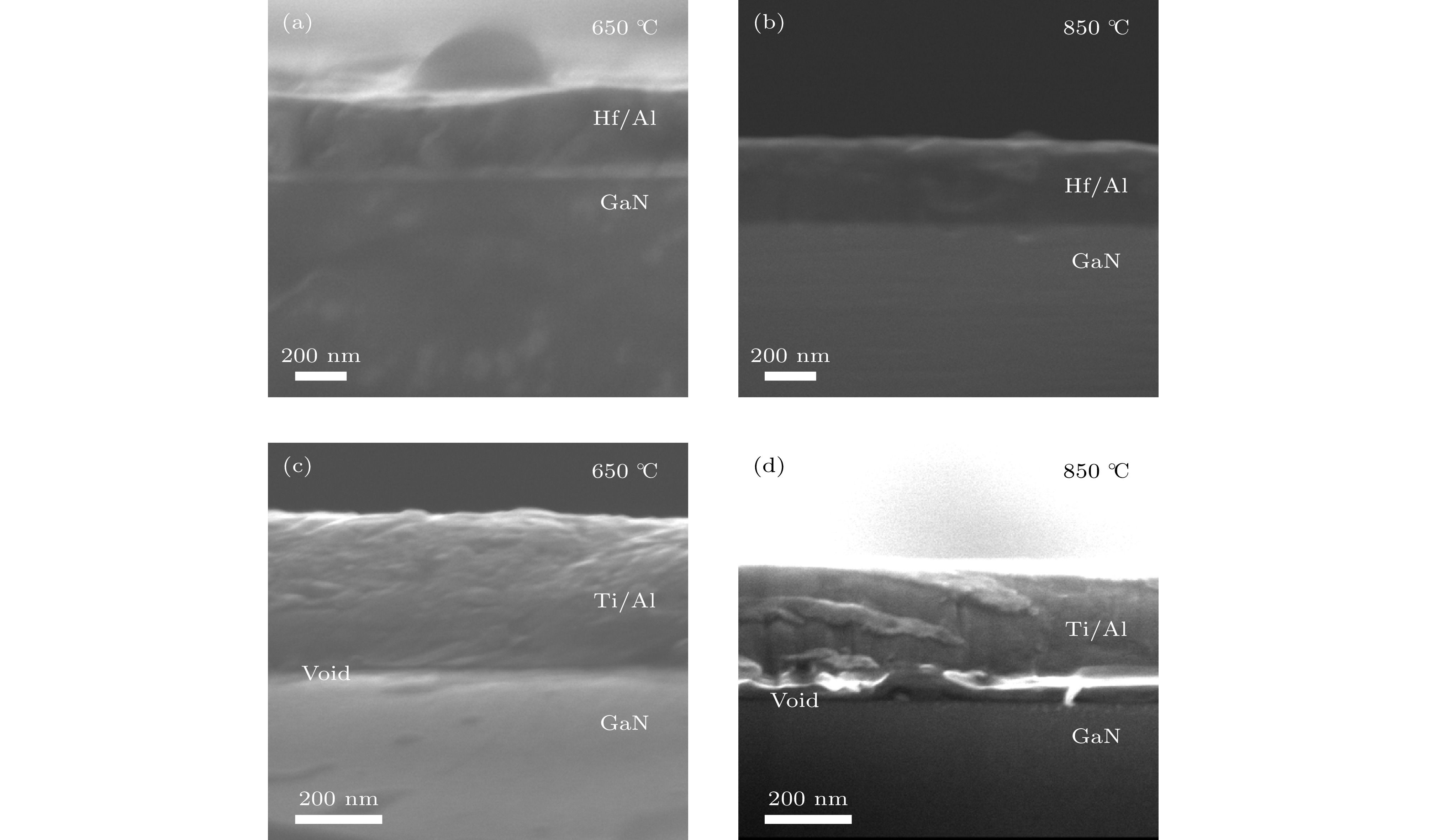 图 5 各电极的截面SEM图像 (a) Hf/Al, 650 ℃; (b) Hf/Al, 850 ℃; (c) Ti/Al, 650 ℃; (d) Ti/Al, 850 ℃
Figure5. Cross-sectional SEM image of each electrode: (a) Hf/Al, 650 ℃; (b) Hf/Al, 850 ℃; (c) Ti/Al, 650 ℃; (d) Ti/Al, 850 ℃
对850 ℃退火条件下的Hf/Al, Ti/Al电极表面进行了SEM表征. 图6为两种电极Hf/Al, Ti/Al的表面SEM图像, 可以看出, 在850 ℃条件下退火的两种电极表面均表现出了颗粒状的形貌, 且在粗糙程度上并没有太大差异. 这与文献中记载的“在高温退火条件下, 电极表面会变得粗糙”表述一致, 这种粗糙的表面对GaN器件的电学性能有一定的影响.
 图 6 各电极在850 ℃条件下退火的表面SEM图 (a) Hf/Al; (b) Ti/Al
Figure6. SEM image of each electrode annealed at 850 ℃ condition: (a) Hf/Al; (b) Ti/Al
