THE EVOLUTION OF INTRAGRANULAR VOIDS UNDER INTERFACE MIGRATION INDUCED BY STRESS MIGRATION
YuWentao*,, HuangPeizhen*, State Key Laboratory of Mechanics and Control of Mechanical Structures, Nanjing University of Aeronautics and Astronautics, Nanjing 210016, China 中图分类号:O343.1 文献标识码:A
关键词:stress migration;interface migration;finite element method;intragranular void evolution;void growth;shrinkage Abstract With the rapid development of microelectronics technology, the failure of interconnects in the integrated circuit raises wide attention. The interconnects inevitably exist some drawbacks, such as voids and cracks. If the drawbacks nucleate, grow and change their shape to form crack-like slits oriented perpendicular to an interconnect line, an open circuit could result. This is a common form of interconnects failure. And interface migration is one of the main mechanisms leading to the evolution of microstructure. Based on the classic theory and weak statement of interface migration, a finite-element method is developed to simulate the evolution of intragranular voids in copper interconnects caused by interface migration induced by stress migration. The validity of the method is confirmed by the agreement of the numerically simulated the undulating surface with that predicted theoretically. Through a large number of numerical simulations, we find that the evolution of the intragranular voids has two trends, namely, void growth and void shrinkage. And the shape of the void is governed by the stress, , the linewidth, , and the initial aspect ratio of the intragranular void, , and there exist critical values for these parameters ( , and ). When , or , the intragranular void will grow along the major axis; otherwise, the intragranular void will shrink into a cylinder. The increase of the stress, or the aspect ratio, or the decrease of the linewidth is beneficial to void growth. And the area of void growth will increase faster with bigger , smaller or bigger . But, the decrease of the stress or the aspect ratio, or increase the linewidth accelerates void shrinkage and the shrinkage area will decrease faster with smaller , bigger or smaller .
为了保证程序计算精度, 定义 作为程序计算误差的衡量标准. 其中 是式(14) 计算得到的解析解, 是本文的有限元解. 取 , 用以表示不同尺寸的模型, 表示程序运行的时间步数. 由于本文所研究的系统应力场变化相对于微结构表面形貌演化的速度慢很多, 即不必微结构表面形貌每更新一次便计算一次应力场. 为保证计算的速度和精确度, 本文微结构形貌更新每隔 步后才计算一次应力场. 图4给出了不同 下误差随时间步数的变化. 可以看到, 误差随着时间步数的增加呈收敛趋势, 且收敛数值小于 3%. 由图可知, 本文取 时可同时保证程序运算的精确度和速度. 显示原图|下载原图ZIP|生成PPT 图4时, 不同 下误差随时间步数的变化. -->Fig.4The error as a function of the time step for different and -->
图6给出了初始形态比不同下晶内孔洞演化生长的临界应力与线宽的关系. 由图可知, 由于线宽直接影响系统的应变能场, 随着线宽增大,表面能逐渐占优, 从而导致 增大. 即同一形态比下, 线宽较小的孔洞更容易长大. 而当线宽较小时, 应变能占优, 临界应力受其影响较大, 变化较快, 此时需特别关注线宽变化对晶内孔洞生长的影响. 在线宽较大时, 临界应力受其影响较小, 曲线变化趋于平缓, 且当线宽时, 可认为线宽变化对晶内孔洞长大的影响可以忽略不计. 显示原图|下载原图ZIP|生成PPT 图6临界应力随线宽 的变化. -->Fig.6The critical value of the stress as a function of the linewidth -->
图7给出了不同应力下孔洞面积变化率随时间的变化. 由图7(a)可知, 在晶内孔洞演化初期的短时间内可能会出现面积减小现象, 而后面积迅速增大; 且应力越小, 面积缩小越明显. 这是因为在较小时孔洞演化前期的表面能占据优势, 晶粒长大, 孔洞收缩; 当孔洞形貌发生一定改变后, 应变能逐渐占据优势, 并一直主导孔洞演化, 促使孔洞长大. 当应力增大到一定程度 时, 应变能始终占优势, 所以未出现面积减小现象. 从曲线上升趋势还可看到, 应力越大, 晶内孔洞生长时面积增大越快. 由图7(b)可知, 当晶内孔洞收缩时, 面积减小非常显著; 且应力越小, 面积减小越快, 更有助于晶内孔洞收缩愈合. 显示原图|下载原图ZIP|生成PPT 图7时面积变化率随时间的变化. -->Fig.7The area change as a function of time for -->
3.2 线宽对晶内孔洞演化的影响
图5(a)和图5(c)给出了和时晶内孔洞的演化. 由图可见, 当时, 由于应变能密度在界面迁移驱动力中占优, 孔洞长大. 当时, 由于表面能占优, 晶粒长大, 孔洞面积收缩并趋于圆形. 同上, 当其他参数不变时, 随着线宽的改变, 孔洞存在生长和收缩两种演化趋势, 且存在一个临界线宽; 当 时, 晶内孔洞在长轴方向长大; 反之, 晶内孔洞收缩并圆柱化. 图8给出了初始应力 不同下晶内孔洞生长的临界线宽 随形态比 的变化. 由图可知, 随着形态比增大而增大, 即同一应力下, 形态比较大的晶内孔洞更容易长大. 在形态比较大时, 应力对临界形态比的影响更为明显, 且孔洞生长的临界线宽随着应力的增大而增大. 在有限元模拟中还发现, 当应力增大到一定值时, 无论线宽如何变化, 对于同一形态比的晶内孔洞都会长大. 这是因为线宽很大时, 其对孔洞表面的应力大小及分布的影响可忽略不计. 显示原图|下载原图ZIP|生成PPT 图8临界线宽和 的关系. -->Fig.8The critical value of the linewidth as a function of -->
图9给出了不同线宽下随时间的变化. 由图可知, 晶内孔洞生长时, 面积总体呈增大趋势. 当时, 在晶内孔洞演化初期的短时间内由于表面能暂时占优, 孔洞面积会出现减小现象, 而后由于应变能逐渐占优导致孔洞面积增大; 且线宽越小, 面积增大越快. 而晶内孔洞缩小时, 线宽越大, 面积减小越快, 有助于晶内孔洞收缩愈合. 显示原图|下载原图ZIP|生成PPT 图9时面积变化随时间的变化. -->Fig.9The area change as a function of time for -->
3.3 形态比对晶内孔洞演化的影响
图5(a)和图5(d)给出了 和 时晶内孔洞的演化图. 由图可见, 当 时, 由于应变能密度在界面迁移驱动力中占优, 孔洞长大. 当 时, 由于表面能占优, 晶粒长大, 孔洞面积收缩并趋于圆形. 同上, 在应力和线宽不变而仅改变形态比时, 晶内孔洞也出现生长和收缩两种演化分叉趋势, 且存在一个临界形态比; 当 时, 晶内孔洞在长轴方向长大; 反之, 晶内孔洞收缩并圆柱化. 图10给出了初始线宽 不同下晶内孔洞生长的临界形态比 随应力 的变化. 由图可见, 随应力增大而减小, 即同一线宽下, 受应力较大的晶内孔洞更易发生扩展. 此外还可看到, 应力较小时, 线宽的变化能显著改变系统的应变能场, 从而显著影响晶内孔洞的演化. 当线宽较大时, 由于表面能占优, 而增大形态比有助于增大应变能, 因而线宽较大的晶内微孔洞扩展所需的临界形态比较大. 显示原图|下载原图ZIP|生成PPT 图10临界形态比和的关系. -->Fig.10The critical value of the aspect ratio as a function of -->
图11给出了不同形态比下孔洞面积随时间的变化. 由图11(a)可见, 晶内孔洞面积总体呈增大趋势. 当时, 在晶内孔洞演化初期的短时间内由于表面能暂时占优, 会出现孔洞面积减小现象. 而后应变能逐渐占优并导致孔洞面积增大; 且形态比越小, 面积减小现象越明显. 从曲线上升趋势还可看到, 形态比越大, 晶内孔洞生长时面积增大越快. 由图11(b)可知, 晶内孔洞收缩时, 形态比越小, 面积减小越快, 有助于孔洞收缩愈合. 显示原图|下载原图ZIP|生成PPT 图11时面积变化随时间的变化. -->Fig.11The area change as a function of time for -->
(FuYunwei, ZhangLong, NiXinhua, et al.Interface cracking analysis with inclusion interaction in composite ceramic .Chinese Journal of Theoretical and Applied Mechanics, 2016,48(1): 154-162 (in Chinese))
[2]
LiuZ, YuH.A numerical study on the effect of mobilities and initial profile in thin film morphology evolution .Thin Solid Films, 2006, 513(1): 391-8
(GengYanan, CaiZongxi.Stability of a pressurized ellipsoidal balloon .Chinese Journal of Theoretical and Applied Mechanics, 2016, 48(5): 1343-1352 (in Chinese))
[4]
XiaL, BowerAF, SuoZ, et al.A finite element analysis of the motion and evolution of voids due to strain and electromigration induced surface diffusion .Journal of the Mechanics & Physics of Solids, 1997, 45(9): 1473-1493
(XiongJun, LiZhenhuan, ZhuYaxin, et al.Microstructure evolution mechanism based crystal-plasticity constitutive modelfor nickel-based superalloy and its finite element simulation .Chinese Journal of Theoretical and Applied Mechanics, 2017, 49(4): 763-781 (in Chinese))
(WuFengshun, ZhangJinsong, WuYiping, et al.Progress of electromigration in IC interconnect metallic line .Semiconductor Technology, 2004, 29(9): 15-21 (in Chinese))
[7]
SuzukiT, NakamuraT, MizushimaY, et al.Stress migration phenomenon in narrow copper interconnects .Journal of Applied Physics, 2007, 101(4): 753
[8]
HoPS.Motion of inclusion induced by a direct current and a temperature gradient .Journal of Applied Physics, 1970, 41(1): 64-68
[9]
HoPS, KwokT.Electromigration in metals .Reports on Progress in Physics, 1989, 52(3): 301
(ZhangJinsong, WuYiping, WangYongguo, et al.Thermomigration in micro interconnects in integrated circuits .Acta Physica Sinica, 2010, 59(6): 4395-4402 (in Chinese))
(GuoJiahui, ZhuLiuhua.The problem about stress migration in the VLSI manufacture .Chinese Journal of Electron Devices, 2000, 23(4): 262-266 (in Chinese))
[12]
GanZH, ShaoW, MhaisalkarSG, et al.Experimental and numerical studies of stress migration in Cu interconnects embedded in different dielectrics .AIP Conference Proceedings, 2006, 817(817): 269-274
(LiuQing, XuKaiyu.Electromigration stress analysis of copper .Chinese Quarterly of Mechanics, 2017(2): 359-368 (in Chinese))
[14]
DongX, LiZ.An analytical solution for motion of an elliptical void under gradient stress field .Applied Physics Letters, 2009, 94, 071909
[15]
WangY, YaoY.A theoretical analysis of the electromigration-induced void morphological evolution under high current density .Acta Mechanica Sinica, 2017, 33: 868-878
[16]
HuangQ, LilleyCM, DivanR.An in situ investigation of electromigration in Cu nanowires .Nanotechnology, 2009, 20(7): 075706
[17]
ManiattyAM, NiJ, LiuY, et al.Effect of microstructure on electromigration-induced stress .Journal of Applied Mechanics, 2016, 83(1): 13-13
[18]
LinSK, LiuYC, ChiuSJ, et al.The electromigration effect revisited: Non-uniform local tensile stress-driven diffusion .Scientific Reports, 2017, 7(1): 3082
[19]
WangH, LiZH, SunJ.Effects of stress and temperature gradients on the evolution of void in metal interconnects driven by electric current and mechanical stress .Modelling & Simulation in Materials Science & Engineering, 2006, 14(4): 607
[20]
HeDN, HuangPZ.A finite-element analysis of intragranular microcracks in metal interconnects due to surface diffusion induced by stress migration .Computational Materials Science, 2014, 87: 65-71
[21]
HeDN, HuangPZ.A finite-element analysis of in-grain microcracks caused by surface diffusion induced by electromigration .International Journal of Solids & Structures, 2015, 62: 248-255
(DuJiefeng, HuangPeizhen.The evolution of intergranular microcracks due to surface diffusion induced by electromigration .Chinese Journal of Solid Mechanics, 2017, 38(1): 39-46 (in Chinese))
[23]
SuoZ.Motions of microscopic surfaces in materials .Advances in Applied Mechanics, 1997, 33(8): 193-294
[24]
SunB, SuoZ, YangW.A finite element method for simulating interface motion—I. Migration of phase and grain boundaries .Acta Materialia, 1997, 45(5): 1907-1915
[25]
HerringC.Surface tension as a motivation for sintering//Fundamental Contributions to the Continuum Theory of Evolving Phase Interfaces in Solids. Berlin, Heidelberg: Springer1999: 33-69
[26]
MullinsWW.Theory of thermal grooving .Journal of Applied Physics, 1957, 28(3): 333-339
[27]
PrevostJH, BakerTJ, LiangJ, et al.A finite element method for stress-assisted surface reaction and delayed fracture .International Journal of Solids & Structures, 2001, 38(30-31): 5185-203
[28]
HuangJM, YangW.Three-dimensional evolution of interfaces under evaporation-condensation kinetics: A finite-element simulation .Modelling & Simulation in Materials Science & Engineering, 1999, 7(1): 87
[29]
YuH.Crack nucleation from a single notch caused by stress-dependent surface reactions .International Journal of Solids & Structures, 2005, 42(13): 3852-3866
[30]
Huang PZ SunJ, LiZH. Evolution of penny-shaped microcracks by interface migration .International Journal of Solids and Structures, 2003, 40(8): 1959-1972
[31]
HuangPZ, SunJ, LiZH.Axisymmetric finite-element simulation of grain growth behaviour .Modelling & Simulation in Materials Science & Engineering, 2002, 11(1): 41
[32]
SrolovitzDJ.On the stability of surfaces of stressed solids .Acta Metallurgica, 1989, 37(2): 621-625
 , 黄佩珍
, 黄佩珍 显示原图|下载原图ZIP|生成PPT
 显示原图|下载原图ZIP|生成PPT
 显示原图|下载原图ZIP|生成PPT
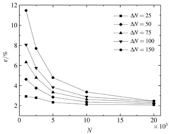 显示原图|下载原图ZIP|生成PPT
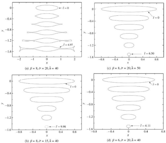 显示原图|下载原图ZIP|生成PPT
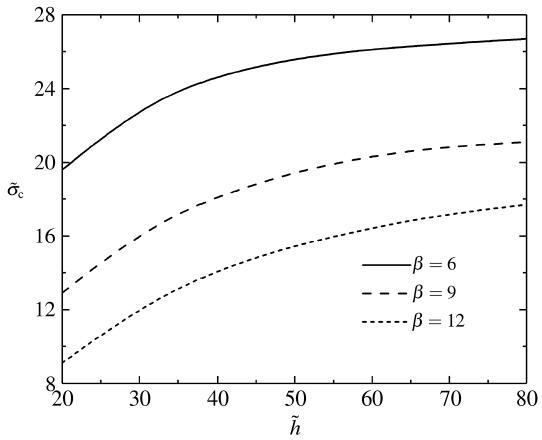 显示原图|下载原图ZIP|生成PPT
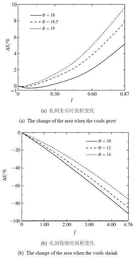 显示原图|下载原图ZIP|生成PPT
 显示原图|下载原图ZIP|生成PPT
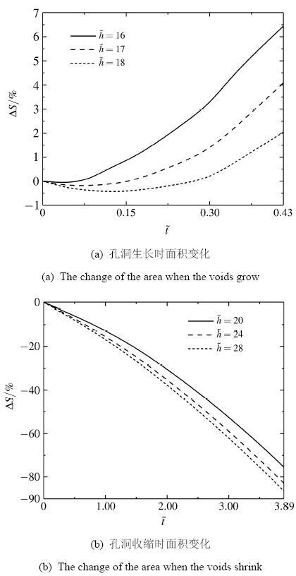 显示原图|下载原图ZIP|生成PPT
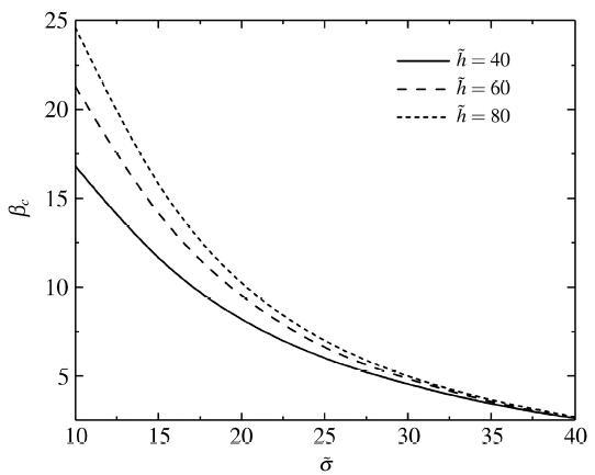 显示原图|下载原图ZIP|生成PPT
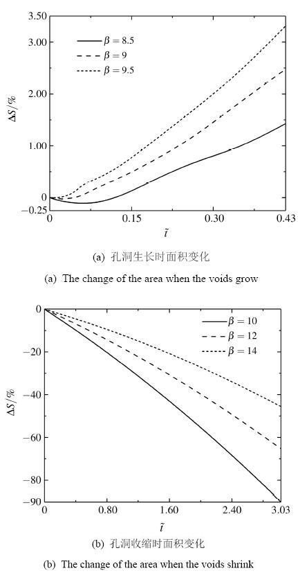 显示原图|下载原图ZIP|生成PPT