全文HTML
--> --> -->不同于STT-MRAM通过改变电流来引入自旋力矩和磁场, 电压调控磁各向异性磁随机存储器(voltage controlled magnetic anisotropy magnetic random access memory, VCMA-MRAM)通过改变外加电压即电场来快速调控磁化方向, 从而有效减小由电流引起的欧姆损耗, 因此具有写入速度快且写入功耗低的显著特点, 有望成为下一代的主流非易失性存储器[11-13]. 而作为构成VCMA-MRAM基本存储单元的磁隧道结(magnetic tunnel junction, MTJ), 现已受到国内外****的广泛关注[14-16]. 近年来, 随着VCMA-MTJ理论的不断深入, 有关****基于VCMA效应建立了VCMA-MTJ的电学模型[17,18], 通过电压来调控MTJ自由层磁化方向, 从而实现数据存储. 然而随着VCMA-MTJ尺寸的不断缩小, 工艺偏差对MTJ性能的影响变得越来越严重, 甚至对VCMA-MTJ电路的读写功能产生了较大影响. 本文在充分考虑磁控溅射(magnetron sputtering)薄膜生长工艺和离子束刻蚀(ion beam etching)工艺会引入工艺偏差的情况下, 给出基于工艺偏差的VCMA-MTJ电学模型, 并研究工艺偏差对VCMA-MTJ自由层磁化方向翻转的影响. 在此基础上, 进一步研究工艺偏差对VCMA-MTJ读写电路中写错误率和读错误率的影响. 本文的研究工作对于VCMA-MTJ器件及其应用电路的设计具有重要的理论和指导意义.
 图 1 VCMA-MTJ结构示意图
Figure1. Schematic structure of the VCMA-MTJ device.
进一步地, VCMA-MTJ在P态和AP态之间的切换与Vb的大小和加载时间密切相关, 下面将结合图2给出的VCMA-MTJ磁化动力学示意图进行分析.
 图 2 VCMA-MTJ的磁化动力学示意图 (a)不同电压对MTJ磁化状态能量势垒的影响; (b)Vb < VC的情况; (c)Vb > VC的情况
Figure2. Illustration of magnetization dynamics for the VCMA-MTJ device: (a) The impacts of different voltages on the energy barrier of MTJ; (b) at a relatively low voltage (Vb < VC); (c) at a high positive voltage (Vb > VC).
从图2(a)中可以看出, VCMA-MTJ在两个稳定磁化状态(P态和AP态)切换时需要克服一定的能量势垒. 该势垒大小受Vb的影响, 当Vb增大时, P态与AP态之间的能量势垒会随之降低, 这有利于VCMA-MTJ的状态切换. 从能量势垒角度来看, 当能量势垒完全消除时, 对应的外加电压称为临界电压(VC).
在图2(b)中, 设参考层磁化方向为z轴正方向且固定不变, 当Vb = 0 V时, 自由层的磁化矢量(M)将围绕有效场(Heff)做强度不变而方向改变的拉莫尔进动, M末端的运动轨迹为一个圆周. 由于自由层M在z轴分量为正, 即与参考层磁化方向平行, 因此VCMA-MTJ将处于P态. 当在t1时刻加载Vb且0 < Vb < VC时, 电荷会在自由层与氧化势垒层接触界面处聚集, 使得垂直磁各向异性发生变化, 导致Heff向x-y平面偏转, 此现象即为电压调控磁各向异性(VCMA)效应[20]. 此时, M将围绕新的Heff方向进动, 并随着时间从t1→t2→t3的增加, M将不断靠近Heff. 由于M在z轴分量始终为正, VCMA-MTJ仍然处于P态, 无法实现VCMA-MTJ状态的切换. 在t4时刻撤除外加电压(Vb = 0 V)后, Heff和M都将返回初始状态, M仍将围绕Heff做强度不变而方向改变的拉莫尔进动, VCMA-MT仍将处于P态.
在图2(c)中, 设参考层磁化方向为z轴正方向且固定不变, 当在t1’时刻加载Vb且Vb ≥ VC时, Heff方向偏转并与x-y平面重合, M将围绕新的Heff方向进动. 在t1’时刻M在z轴的分量为正, VCMA-MTJ处于P态. 在t2’时刻M在z轴的分量变为负, 此时VCMA-MTJ将由P态切换到AP态. 进一步, 随着时间从


设m为自由层磁化矢量方向上的单位向量, 则有M = MS·m, 且m在直角坐标系中可表示为
当考虑外加电压Vb对有效磁场Heff的影响时, Heff可具体表示为[22]
可以看出, Hk与外加电压Vb有关, 可进一步表示[23]为
同时, 设参考层磁化方向为z轴正方向且固定不变, 则m还可表示为
将(2)—(5)式带入(1)式, 求解得到
进一步地, 通过求解θ即mz = cosθ来确定VCMA-MTJ的磁化状态. 本文中VCMA-MTJ模型用到的部分参数[17,18]如表1所示.
| 参数 | 符号 | 数值 | 单位 |
| 氧化势垒层厚度标准值 | tox | 1.4 | nm |
| 垂直磁各向异性系数 | Ki | 0.32 | mJ/m2 |
| 电压调控磁各项异性系数 | ξ | 60 | fJ/(V·m) |
| 自由层厚度标准值 | tf | 1.1 | nm |
| 简化的旋磁比 | γ | 2.21 × 10⁵ | m/(A·s) |
| 磁导率 | μ0 | 1.256 × 10⁻⁶ | H/m |
| 吉尔伯特阻尼因子 | αd | 0.05 | |
| 饱和磁化强度 | Ms | 0.625 × 10⁶ | A/m |
| x, y 轴退磁因子 | Nx, y | 0.0168 | |
| z 轴退磁因子 | Nz | 0.966 | |
| 外加磁场在 x 轴分量 | Hx | 31830 | A/m |
表1VCMA-MTJ模型参数列表
Table1.Parameters of the VCMA-MTJ model.
图3给出了VCMA-MTJ自由层磁化矢量在z轴分量(即mz)随时间的变化曲线, 并分析了Vb对磁化状态切换的影响. 从图3可以看出, 在恒定的外加电压脉冲宽度(tpw = 0.4 ns)下, 当Vb ≤ 0.9 V时, mz始终为正, VCMA-MTJ磁化状态保持不变, 始终处于初始态P态; 当Vb ≥ 1.0 V时, 随着时间的增加, mz将由正变负, 即磁化状态发生改变, VCMA-MTJ将由初始的P态切换为AP态. 同时, 将mz首次经由1降低至–0.95所持续的时间定义为VCMA-MTJ的切换速度(tsw), 则Vb = 1.0 V, tpw = 0.4 ns时对应的tsw为1.25 ns.
 图 3 VCMA-MTJ磁化状态随时间的变化曲线, 其中插图是切换速度的定义
Figure3. Magnetization state versus time of VCMA-MTJ, the inset represents the definition of the switching speed.
图4进一步给出了tsw随Vb的变化曲线. 从图4可以看出, 在tpw = 0.4 ns时, 当Vb ≤ 1.3 V时, tsw随Vb的增加呈显著下降趋势; 当Vb > 1.3 V时, Vb对tsw的影响不大, tsw几乎保持不变. 通过拟合可以看出, tsw与Vb近似呈e指数关系.
 图 4 不同Vb对VCMA-MTJ磁化状态切换速度的影响, 其中tpw = 0.4 ns
Figure4. Effect of Vb on the magnetization direction switching speed of VCMA-MTJ at tpw = 0.4 ns.
图5给出了tpw对VCMA-MTJ磁化状态切换的影响. 从图5可以看出, 在恒定的外加电压(Vb = 1.2 V)下, 当tpw ≤ 0.1 ns时, mz始终为正, VCMA-MTJ磁化状态保持不变, 始终处于初始态P态; 当0.2 ns ≤ tpw ≤ 0.6 ns时, 随着时间的增加, mz将由正变负, 即磁化状态发生改变, VCMA-MTJ将由初始的P态切换为AP态. 当tpw进一步增大(例如tpw = 0.8 ns)时, 在拉莫尔进动过程中随着时间从

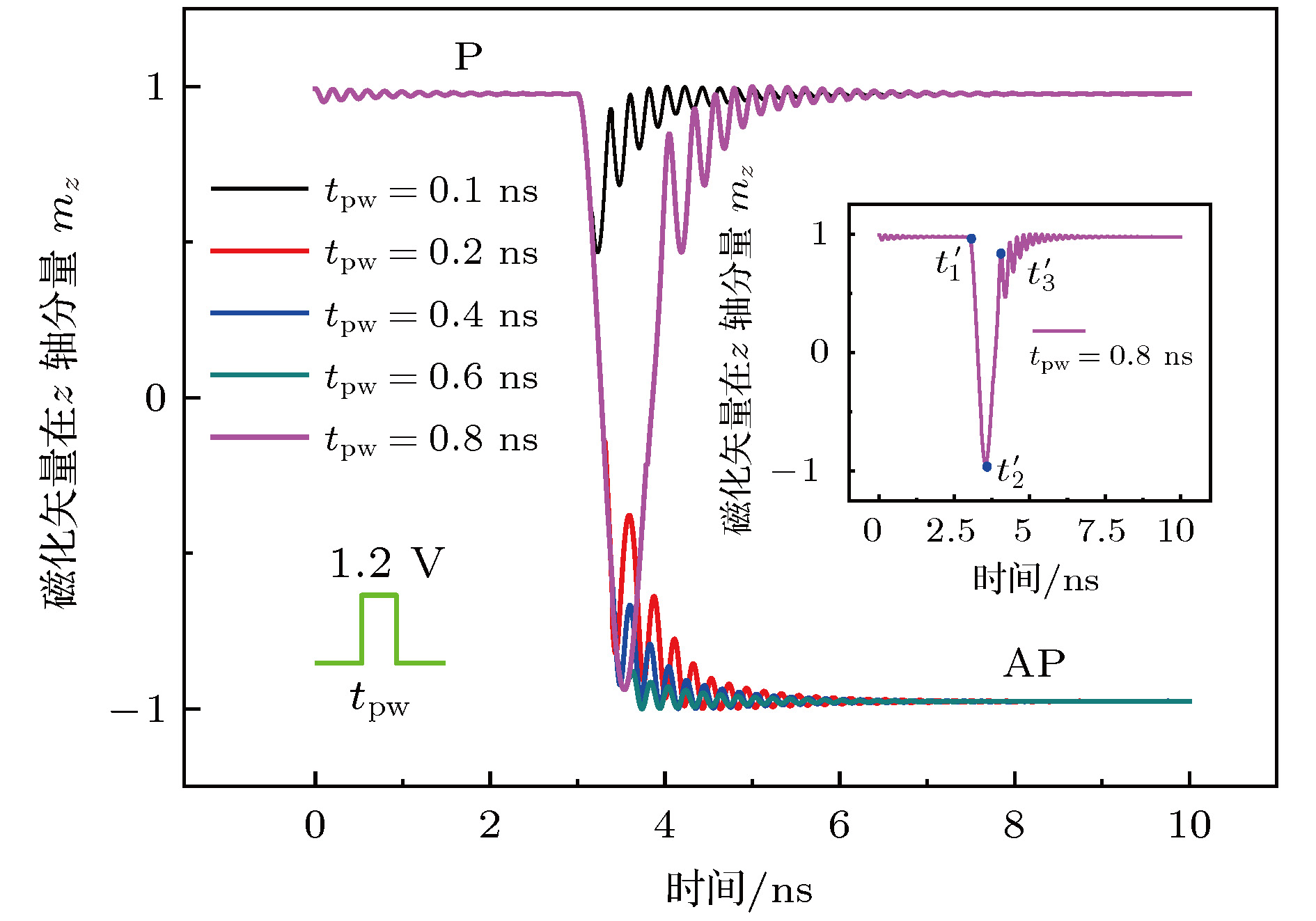 图 5 不同tpw对VCMA-MTJ磁化状态切换的影响, 插图为与图2(c)相对应的mz变化情况
Figure5. Effect of tpw on the magnetization direction switching of VCMA-MTJ, the inset shows the precession of mz corresponding to Fig. 2(c).
2
3.1.薄膜生长工艺偏差的影响
VCMA-MTJ的典型制备工艺主要包括薄膜生长、热退火及刻蚀工艺. 其中VCMA-MTJ中自由层、氧化势垒层和参考层大都是采用磁控溅射法[24,25]制备得到, 该方法具有薄膜沉积速度快、适用于多种材料混合溅射、可实现大批量生产等优点. 然而在薄膜生长过程中, 薄膜厚度会不可避免地存在几个原子层厚度范围内的微小偏差[26,27], 如图6所示, 其中tox0和tox1分别为氧化势垒层厚度的最大值和最小值, tf0和tf1分别为自由层厚度的最大值和最小值, toxm和tfm分别为考虑薄膜厚度偏差情况下氧化势垒层厚度和自由层厚度的等效均值. 随着VCMA-MTJ尺寸的不断缩小, 上述薄膜厚度偏差将会对器件的磁化翻转产生重要的影响. 图 6 薄膜生长工艺产生的厚度偏差示意图
Figure6. Schematic illustration of thickness deviation caused by the thin film growth process.
考虑到垂直磁各向异性主要来源于自由层和氧化势垒层之间的界面相互作用, 垂直磁各向异性对自由层厚度和氧化势垒层厚度的变化更为敏感[28]. 本文采用自由层厚度偏差(γtf)和氧化势垒层厚度偏差(γtox)来具体表征在磁控溅射工艺生长薄膜中产生的厚度偏差. 此时, 可分别表示为
此时, 垂直磁各向异性场Hk可表示为
图7给出了不同γtf对VCMA-MTJ磁化状态切换的影响, 其中Vb = 1.2 V, tpw = 0.4 ns. 当γtf ≤ 12%时, MTJ自由层的磁化方向能够实现从P态到AP态的切换; 当γtf ≥ 13%时, MTJ不能实现从P态到AP态的切换. 这是因为, 从(9)式可知, 随着γtf的增加, Hk将减小, 从而导致MTJ的Heff向x-y平面偏转, 这不利于磁化方向的有效翻转.
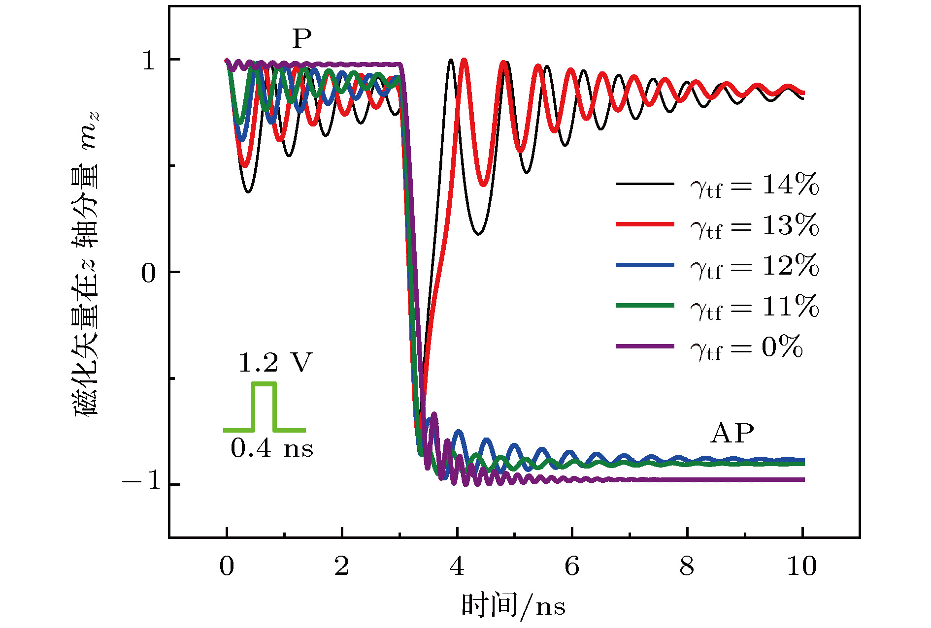 图 7 γtf对VCMA-MTJ磁化方向切换的影响, 其中Vb = 1.2 V, tpw = 0.4 ns
Figure7. Effect of γtf on the magnetization direction switchingof VCMA-MTJ at Vb = 1.2 V, tpw = 0.4 ns.
图8给出了不同γtox对VCMA-MTJ磁化状态切换的影响. 当γtox ≤ 10%时, 自由层的磁化矢量能够发生翻转, VCMA-MTJ将由初始的P态切换为AP态; 当γtox ≥ 11%时, VCMA-MTJ将无法实现磁化状态的切换. 这是因为, 从(10)式可知, 当γtox较大时, 临界电压VC增大, 进而影响了自由层磁化矢量的进动, 从而导致切换错误.
 图 8 不同γtox对VCMA-MTJ磁化状态切换的影响, 其中Vb = 1.1 V, tpw = 0.4 ns
Figure8. Effect of γtox on magnetization direction switching of VCMA-MTJ at Vb = 1.1 V and tpw = 0.4 ns.
2
3.2.刻蚀工艺
离子束刻蚀技术具有刻蚀速率快、图形精度高、工艺参数可控性好等优势, 因此成为MTJ刻蚀的主流工具[29-31]. 但离子束刻蚀不可避免地会产生具有磁性的非挥发刻蚀产物, 如果沟槽深度较大或者沟槽宽度较小, 则粒子不能全部飞出槽外, 导致部分粒子附着在侧壁上, 形成再沉积层[32,33](图9).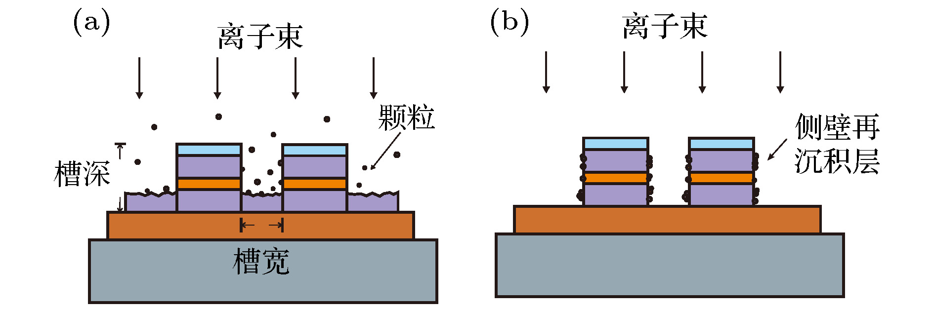 图 9 离子束刻蚀产生侧壁再沉积层示意图 (a)刻蚀产生磁性粒子; (b)粒子聚集形成再沉积层
Figure9. Illustration of the formation of the sidewall re-deposited layer with ion beam etching: (a) Producing of magnetic particleses with etching process; (b) formation of the re-deposition layer with magnetic particleses.
由于侧壁再沉积层引入的磁性会干扰自由层的垂直磁各向异性场[34], 因而需要考虑再沉积层对自由层磁性的影响. 此时, 有效的垂直磁各向异性场可表示为
图10给出了不同α对VCMA-MTJ磁化状态切换的影响. 当0.8 ≤ α ≤ 1时, 自由层的磁化方向可以实现稳定的翻转; 当α ≤ 0.7时, 磁化方向的进动过程变得紊乱. 这是因为随着α的减小, Hk将呈指数式减小, 即再沉积层的存在显著降低了垂直磁各向异性, 使得有效磁场的垂直方向发生偏移, 稳定性降低, 此时VCMA-MTJ的自由层磁化方向在翻转的过程中更易受到温度相关因素的干扰.
 图 10 不同α对VCMA-MTJ磁化方向切换的影响
Figure10. Effect of α on magnetization direction switching of VCMA-MTJ.
综上所述, 工艺偏差的存在使得VCMA-MTJ自由层磁化方向的翻转变得不确定, 从而影响到VCMA-MTJ读写电路数据存储的正确性. 下面将采用上述电学模型来分析工艺偏差对VCMA-MTJ读写电路错误率的影响.
 图 11 VCMA-MTJ读写电路
Figure11. Reading and writing circuit of VCMA-MTJ.
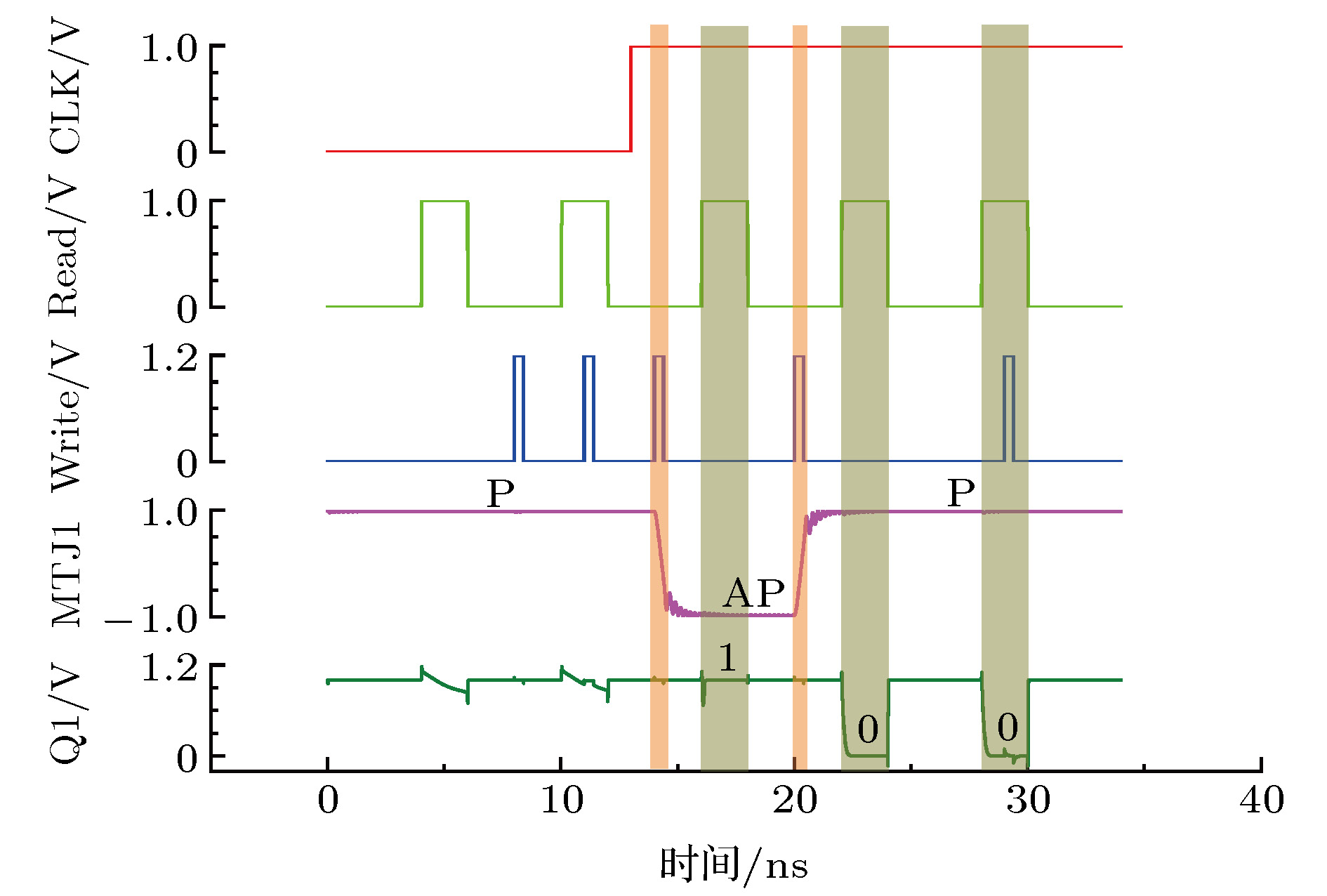 图 12 VCMA-MTJ读写电路的仿真波形
Figure12. Simulation waveform of the reading and writing circuit of VCMA-MTJ.
当CLK为高电平“1”时, N4, N5导通. 若Read为“0”, 则N2, N3关断, N4导通. 此时当Write为“1”时, 进行写操作, MTJ1从P态变为AP态, 存入数据“1”.
由于Read为“0”, P0, P1, P2和P3导通, 且N2, N3关断, Vdd将Q0, Q1上拉到高电平, N0, N1导通. 若此时Read变为“1”, 则P0, P3关断, N2, N3导通, 上述电路通过比较MTJ1和MTJ0的阻值来进行读操作, 共有两种情况: 1)当MTJ1存储数据为“1”时, 呈AP态, 其电阻(R1)大于MTJ0的电阻(R0), 此时Q0电位下降速度快于Q1, 相应地, P1早于P2导通, Q1将由Vdd上拉到高电平, 输出“1”, 实现读操作; 2)当MTJ1存储数据为“0”时, 呈P态, 即R1小于R0, 此时Q1电位下降速度快于Q0, 相应地, P2早于P1导通, Q0将由Vdd上拉到高电平, N0持续导通, 使得Q1输出“0”, 实现读操作.
现今, 基于自旋转移力矩磁隧道结(spin-transfer torque-magnetic tunnel junction, STT-MTJ)的MRAM存储容量已高达1 GB[36], 此时工艺偏差对MTJ的影响将变得越来越严重. 本文以VCMA-MTJ为研究对象, 重点研究了工艺偏差对器件几何参数(包括tf, tox, α)及其所在读写电路特性的影响. 通常在考虑工艺偏差影响的情况下, 可认为MRAM中VCMA-MTJ的tf, tox和α遵循高斯分布[37], 即
2
4.1.写错误率
图13给出了VCMA-MTJ读写电路在进行写“1”操作时的蒙特卡洛仿真波形, 其中N = 100, 3σ/μ = 0.03, Vb = 1.2 V, tpw = 0.4 ns. 结果表明, 由于工艺误差的影响, 4%的VCMA-MTJ未能实现磁化方向的翻转而出现写错误, 即写错误率为4%.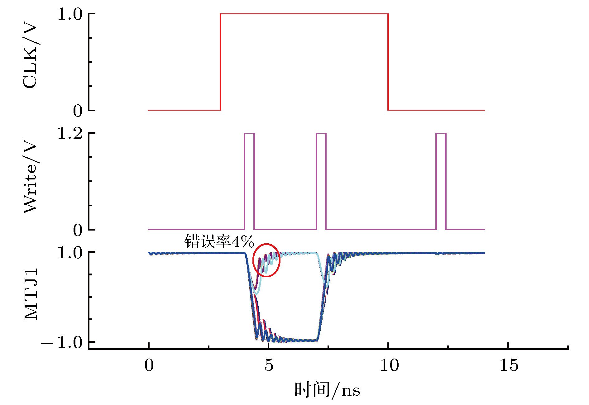 图 13 VCMA-MTJ写电路的蒙特卡洛仿真波形, 其中N = 100, 3σ/μ = 0.03, Vb = 1.2 V, tpw = 0.4 ns
Figure13. Monte Carlo simulation waveform of the writing circuit of VCMA-MTJ at N = 100, 3σ/μ = 0.03, Vb = 1.2 V, tpw = 0.4 ns.
图14给出了不同Vb下写错误率随3σ/μ的变化关系曲线. 从图14可以看出, 写错误率均随着3σ/μ的增大而增大, 适当增大Vb可显著降低写错误率. 当Vb = 1.3 V, 3σ/μ增大为0.05时, 写错误率为0%, 远低于Vb = 1.15 V, 3σ/μ = 0.05时的写错误率(30%).
 图 14 不同Vb下写错误率随3σ/μ的变化关系
Figure14. Writing error rate versus 3σ/μ at different Vb
图15给出了不同tpw下写错误率随3σ/μ的变化关系曲线. 从图15可以看出, 写错误率均随着3σ/μ的增大而增大, 适当减小tpw可显著降低写错误率. 当tpw = 0.5 ns, 3σ/μ = 0.05时, 写错误率仅为15%, 远低于tpw = 0.8 ns, 3σ/μ = 0.05时的写错误率(42%).
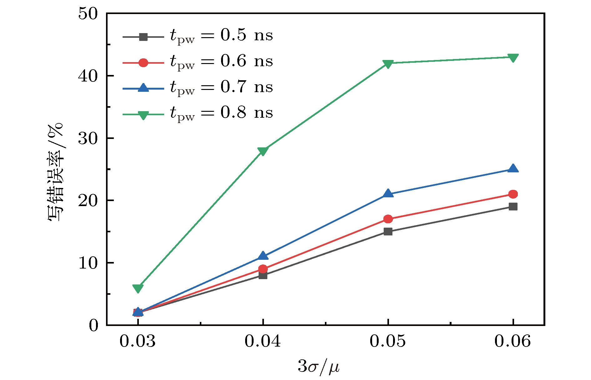 图 15 不同tpw下写错误率随3σ/μ的变化关系
Figure15. Writing error rate versus 3σ/μ at different tpw.
2
4.2.读错误率
图16给出了VCMA-MTJ读写电路在进行读“0”操作时的蒙特卡洛仿真波形, 其中N = 100, 3σ/μ = 0.07, Vdd = 0.8 V. 结果表明, 由于工艺误差的影响, 读错误率为2%. 图 16 VCMA-MTJ读电路的蒙特卡洛仿真波形, 其中N = 100, 3σ/μ = 0.07, Vdd = 0.8 V
Figure16. Monte Carlo simulation waveform of the reading circuit of VCMA-MTJ at N = 100, 3σ/μ = 0.07, Vdd = 0.8 V
图17给出了不同Vdd下VCMA-MTJ读写电路发生读操作错误时读错误率随3σ/μ变化的关系曲线, 上述读写电路中N = 100. 从图17可以看出, 读错误率均随着3σ/μ的增大而增大, 适当增大Vdd可显著降低读错误率. 在相同3σ/μ = 0.07下, 当Vdd = 0.9 V时, 读错误率为0%, 远低于Vdd = 0.6 V时的读错误率(31%). 然而增大Vdd会增加读写电路的功耗, 需要折中考虑.
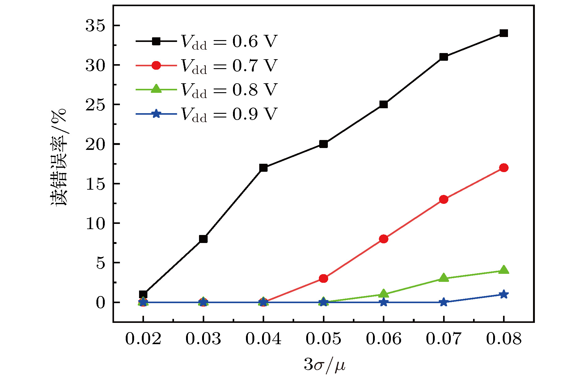 图 17 不同Vdd下读错误率随3σ/μ的变化关系
Figure17. Reading error rate versus 3σ/μ at different Vdd.
