
 , ZHENG Qingrong1

1. School of Physical Sciences, University of Chinese Academy of Sciences, Beijing 100049, China;
2. Key Laboratory of Micro-Nano Measurement-Manipulation and Physics of Ministry of Education, Department of Physics, Beihang University, Beijing 100191, China
Received 26 March 2019; Revised 8 May 2019
Foundation items: Supported by the National Natural Science Foundation of China(11574309, 11504013)
Corresponding author: SHENG Xianlei, E-mail: xlsheng@buaa.edu.cn
ZHENG Qingrong, E-mail: qrzheng@ucas.ac.cn
Abstract: Based on the first-principle calculations, we propose that the monolayer VCl3 and VBr3 are quantum anomalous Hall insulators with in-plane magnetization without considering the correlation effect of the 3d electron-electron interaction. The band gap is predicted to be about 3.4 meV for VCl3, but no global gap for VBr3. It is interesting to note that VCl3 (VBr3) possesses a Chern number of C=3 (C=1) with three (one) chiral edge states. After considering correlation effect, we obtain Mott insulator if U>0.45 (U>0.35) eV for VCl3 (VBr3).
Keywords: ferromagnetic semiconductorlarge Chern numberMott insulator
单层VCl3和VBr3中相互作用导致的量子反常霍尔绝缘体到莫特绝缘体相变
徐永峰1, 胜献雷2

 , 郑庆荣1

1. 中国科学院大学物理科学学院, 北京 100049;
2. 北京航空航天大学物理系 微纳测控与低维物理教育部重点实验室, 北京 100191
摘要: 基于第一性原理计算,发现在不考虑3d电子间关联作用的情况下,二维单层材料VCl3和VBr3是面内铁磁半导体,并且具有量子反常霍尔效应。VCl3能隙约为3.4 meV,VBr3没有全局的能隙。有趣的是,VCl3的陈数为3,有3个手性边缘态;VBr3的陈数为1,对应1个手性边缘态。当考虑关联作用U后,它们会变为Mott绝缘体。对于VCl3,相变点发生在U=0.45 eV;对于VBr3,相变点发生在U=0.35 eV。
关键词: 铁磁半导体大陈数Mott绝缘体
Since the discovery of quantum Hall (QH) effect, the study of the topological phase of matter has attracted great attention in the condensed-matter community. A voltage caused by the deflected motion of charged particles under external electric field and magnetic field leads to the quantized Hall conductance [1]. Nevertheless, the quantum Hall effect may be achieved without external magnetic field. In 1988, Haldane[2] proposed the quantum anomalous Hall (QAH) effect in a two-dimensional (2D) honeycomb lattice with next-nearest-neighboring hopping modulated by staggered flux. Dissipative boundary states exist in the two edges of materials with QAH effect[3-5]. The anomalous Hall effect has an intrinsic origin due to spin-dependent band structure of conduction electrons, which can be expressed in terms of the Berry phase or Chern number in the momentum space[6]. This effect originates from the coupling of electron orbital motion to its spin, i.e., spin orbit coupling (SOC), resulting in the opposite motion of electrons with spin-up and spin-down. In a ferromagnetic metal, the magnetization causes an imbalance in the population between the electrons with spin-up and spin-down and consequently leads to the anomalous Hall effect. Considering the time reversal (TR) symmetry, the quantities of electrons moving in the opposite directions with different spins are equal and as a result there is no charge Hall conductance, but a nonzero spin Hall conductance exhibits quantum spin Hall (QSH) effect[7]. The QAH insulator[8] was a recently discovered topological electronic phase where strong SOC and ferromagnetic ordering conspire to generate a band gap Eg in the bulk of a two-dimensional (2D) electron system, as well as conducting gapless chiral edge states in its boundaries. The edge states are robust against impurities or disorders because the electron backscattering in the two edge channels is prohibited due to the TR symmetry. Topologically nontrivial band structure is characterized by a nonzero Chern number by counting the number of edge states. The QAH effect not only occurs in out-of-plane magnetization systems[9-15], but also exists in in-plane magnetization materials[16-21].
The layered transition-metal trichlorides materials of MCl3 (M=Ti, V, Cr, Fe, Mo, Ru, Rh, Ir) have been achieved for many years due to relatively weak van der Waals interaction between the interlayers [22-25]. These layered materials, which possess honeycomb lattice, partially occupied d-orbitals, and nonnegligible SOC, may have interesting properties, and thus they are worth studying.
1 Computational methodsThe first-principle calculations were performed within the Vienna ab initio simulation package (VASP) using the projector augmented wave (PAW) method in the framework of density functional theory (DFT)[26-28]. The electron exchange correlation functional was described by the generalized gradient approximation (GGA) in the form proposed by Perdew, Burke, and Ernzerhof (PBE)[29]. The lattice parameters are chosen from Springer Materials[30]. The structure relaxation considering both the atomic positions and lattice vectors was performed by the conjugate gradient (CG) scheme until the maximum force on each atom was less than 0.01eV/?(1?=0.1nm), and the total energy converge threshold was 10-6eV with Gaussian smearing method. To avoid unnecessary interactions between the monolayer and its periodic images, the vacuum layer was set as 20?. The energy cut off of the plane waves was chosen as 520eV. The Brillouin zone (BZ) integration was sampled with a 9×9×1 G-centered Monk horst Pack grid. The relaxed lattice parameter (a=6.012?) was adopted in the calculations. SOC is included by a second variational procedure on a fully self-consistent basis. An effective tight binding Hamiltonian based on the maximally localized Wannier functions (MLWF) was used to investigate the surface states[21, 31]. The iterative Greens function method[32] was used with the package WannierTools[33].
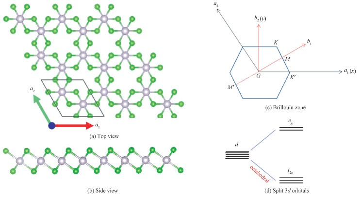
2 Results and discussionThe two-dimensional VCl3 (VBr3) consists of a V atomic layer sandwiched by two Cl atomic layers. The V atoms form a honeycomb lattice and each V atom is surrounded by six Cl atoms, which forms an octahedral crystal field, as shown in Fig. 1. It takes the same structure as monolayer OsCl3 that has been shown to be an intrinsic quantum anomalous Hall insulator[34]. V is a transition metal element with partially filled 3d-orbitals, which may result in magnetism. Based on the first-principle calculations, we consider several magnetic configurations, including ferromagnetic (FM), antiferromagnetic (AFM), and paramagnetic (PM) states. We firstly take VCl3 as an example and find that VCl3 takes the FM ground state with in-plane magnetization along zigzag direction as shown in Table 1.
Fig. 1
 | Download: JPG larger image |
Fig. 1 Top (a) and side (b) views of monolayer VCl3, first Brillouin zone(c) of monolayer VCl3 with direct reciprocal lattice vectors and the high symmetry points indicated, and 3d orbital splitting under octahedral crystal field (d) | |
Table 1
| Table 1 FM and AFM energies of VCl3 | ||||||||||||||||||||||||||||||||||||||||
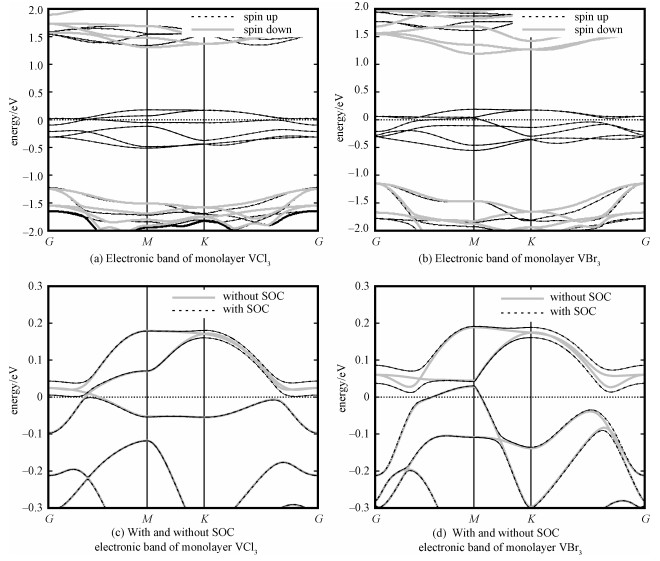
The band structure calculations show that VCl3 is a fully spin-polarized half metal. Without considering SOC, it is a 2D Weyl half semimetal with a band crossing point in each G-M path, such that there are total 6 Weyl points in the first BZ. After turning on SOC, a band gap of about 3.4meV was opened, and the material becomes a ferromagnetic semiconductor, which is different from PtCl3 which is a 2D Weyl half semimetal even with SOC due to additional symmetry protection[35]. To understand these features, we find that under the octahedral crystal field formed by Cl atoms, V-3d orbitals are split into t2gand eg orbital groups, and the latter is higher in energy. For each V3+ with two valence electrons, there are four valence electrons in one primitive cell, such that V-t2g orbitals will be partially filled in one spin channel. The other t2g spin channel and all eg orbitals are empty. Therefore, the system is half Weyl semimetal without considering SOC. If turning on SOC, the t2g orbitals will split into j=1/2 doublet state and j=3/2 quartet state with the former energetically higher, such that the system becomes a semiconductor, as shown in Fig. 2. The topologically nontrivial band structure of VCl3 may come from the combination effect of honeycomb lattice formed by V atoms and the SOC of transition metal V atoms.
Fig. 2
 | Download: JPG larger image |
Fig. 2 Electronic band structures of monolayer VCl3 and VBr3 | |
Furthermore, because of the ferromagnetic ordering of the magnetic moments in V atoms, the system results in a quantum anomalous Hall insulator. To show the topology, we calculated the gauge-invariant Berry curvature in momentum space. The Berry curvature Ωz(k) in 2D can be obtained by analyzing the Bloch wave functions from the self-consistent potentials
| ${\Omega _z}\left( k \right) = {\sum _n}f_n^z{\Omega _n}\left( k \right), $ | (1) |
| $\begin{array}{l}\Omega _n^z\left( k \right) = - 2{\sum _{m \ne n}}{\rm{Im}}\\{\rm{ }}\frac{{\left\langle {{\psi _n}\left( k \right)\left| {{v_x}} \right|{\psi _m}\left( k \right)} \right\rangle \left\langle {{\psi _m}\left( k \right)\left| {{v_y}} \right|{\psi _n}\left( k \right)} \right\rangle }}{{{{\left( {{\varepsilon _n}\left( k \right) - {\varepsilon _m}\left( k \right)} \right)}^2}}}, \end{array}$ | (2) |
| $C = \frac{1}{{2{\rm{ \mathsf{ π} }}}}\int {{\rm{d}}{k^2}{\Omega _z}(k)} .$ | (3) |
 | Download: JPG larger image |
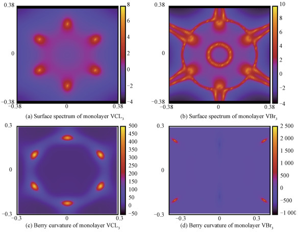
Fig. 3 Surface spectra of monolayer VCl3 at energy level 0.01eV (a) and monolayer VBr3 at energy level 0.07eV (b), and Berry curvature of monolayer VCl3 and VBr3 in the BZ (c, d) | |
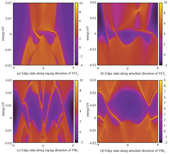
Two Berry curvature peaks contribute to the nonzero Chern number 1 and consequently the total Chern number is 3 by integrating the Berry curvature in the whole BZ. According to the bulk-edge correspondence[36], the nonzero Chern number is closely related to the number of nontrivial chiral edge states that emerge inside the bulk gap of a semi-infinite system. With an effective concept of principle layers, an iterative procedure to calculate the Greens function for a semi-infinite system is employed. The momentum and energy dependence of the local density of states at the edge can be obtained from the imaginary part of the surface Greens function
| $A\left( {k, \omega } \right) = - \frac{1}{{\rm{ \mathsf{ π} }}}\mathop {{\rm{lim}}}\limits_{\eta \to {0^ + }} {\rm{ImTrGs}}\left( {k, \omega + {\rm{i}}\eta } \right), $ | (4) |
Fig. 4
 | Download: JPG larger image |
Fig. 4 Energy and k-dependence of the local DOS on the edge of the semi-infinite sheet of VCl3 (a, b) and VBr3(c, d) | |
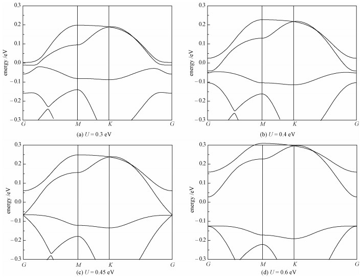
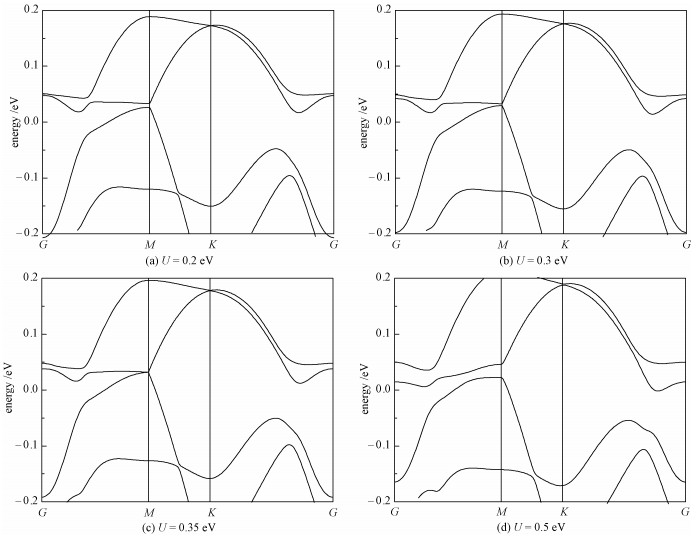
As shown in Fig. 5 (Fig. 6), the change of band structure as a function of correlation strength U for monolayer VCl3 (VBr3)indicates that there exits a phase transition at U≈0.45eV (0.35eV), and stronger correlation will turn it into a Mott insulator. We also calculated the properties of a monolayer VBr3. Although the monolayer VBr3 exhibits some similar properties as in VCl3, i.e., a Weyl semimetal without SOC (Fig. 2(b)) and an energy gap is opened when including SOC (Fig. 2(d)), the monolayer VBr3 has the total Chern number C=1 from 6 Berry curvature peaks, of which 4 peaks have positive sign and 2 peaks have negative sign (Fig. 3(d)). The nonzero Chern number 1 corresponds to one gapless chiral edge state (Fig. 4(b) and 4(d)) connecting the valence and conduction bands.
Fig. 5
 | Download: JPG larger image |
Fig. 5 Electronic band structure of monolayer VCl3 with ferromagnetic momentum 4μB per unit cell along the zigzag direction at different correlation energy values | |
Fig. 6
 | Download: JPG larger image |
Fig. 6 Electronic band structure of monolayer VBr3 with ferromagnetic momentum 4μB per unit cell along the zigzag direction at different correlation energy values | |
3 DiscussionIn summary, based on the first-principle calculations, we propose that the 2D monolayer VCl3 and VBr3 are QAH insulators without considering correlation effect, and they transform into Mott insulators after turning on the correlation effect U. At the mean-field theory level, VCl3 and VBr3 exhibit QAH insulating states with Chern numbers of 3 and 1, respectively, thus giving rise to chiral gapless edge states. If the correlation U is larger than about 0.45 (0.35)eV for VCl3 (VBr3), it will cause a topological phase transition and the monolayer turns into a Mott insulator. These topological properties can be detected by electrical transport experiment, which has been carried out in detecting the QAHE in V-doped (Bi, Sb)2Te3 thin film [37], Cr/V-codoped (Bi, Sb)2Te3 system[38], and other doped TIs [39].
The authors thank YOU Jingyang for helpful discussion.
References
| [1] | Hall E H. On a new action of the magnet on electric currents[J]. American Journal of Mathematics, 1879, 2(3): 287. DOI:10.2307/2369245 |
| [2] | Haldane F D M. Model for a quantum hall effect without landau levels:condensed-matter realization of the "parity anomaly"[J]. Physical Review Letters, 1988, 61(18): 2015-2018. |
| [3] | Weng H M, Yu R, Hu X, et al. Quantum anomalous hall effect and related topological electronic states[J]. Advances in Physics, 2015, 64(3): 227-282. DOI:10.1080/00018732.2015.1068524 |
| [4] | Liu C X, Zhang S C, Qi X L. The quantum anomalous Hall effect:theory and experiment[J]. Annual Review of Condensed Matter Physics, 2016, 7(1): 301-321. DOI:10.1146/annurev-conmatphys-031115-011417 |
| [5] | Ren Y F, Qiao Z H, Niu Q. Topological phases in two-dimensional materials:a review[J]. Reports on Progress in Physics, 2016, 79(6): 066501. DOI:10.1088/0034-4885/79/6/066501 |
| [6] | Nagaosa N, Sinova J, Shigeki O, et al. Anomalous Hall effect[J]. Reviews of Modern Physics, 2010, 82(2): 1539-1592. DOI:10.1103/RevModPhys.82.1539 |
| [7] | Kane C L, Mele E J. Quantum spin Hall effect in graphene[J]. Physical Review Letters, 2005, 95(22): 226801. DOI:10.1103/PhysRevLett.95.226801 |
| [8] | Kou X F, Fan Y B, Lang M R, et al. Magnetic topological insulators and quantum anomalous Hall effect[J]. Solid State Communications, 2015, 215-216: 34-53. DOI:10.1016/j.ssc.2014.10.022 |
| [9] | Chun S H, Chai Y S, Yoon S O, et al. Realization of giant magnetoelectricity in helimagnets[J]. Physical Review Letters, 2010, 104(03): 037204. DOI:10.1103/PhysRevLett.104.037204 |
| [10] | Qiao Z H, Yang S Y, Feng W X, et al. Quantum anomalous Hall effect in graphene from Rashba and exchange effects[J]. Physical Review B, 2010, 82(16): 161414. DOI:10.1103/PhysRevB.82.161414 |
| [11] | Tse W K, Qiao Z H, Yao Y G, et al. Quantum anomalous Hall effect in single-layer and bilayer graphene[J]. Physical Review B, 2011, 83(15): 155447. DOI:10.1103/PhysRevB.83.155447 |
| [12] | Xu G, Weng H M, Wang Z J, et al. Chern semimetal amd the quantized amomalous Hall effect in HgCr2Se4[J]. Physical Review Letters, 2011, 107(18): 186806. DOI:10.1103/PhysRevLett.107.186806 |
| [13] | Yu R, Zhang W, Zhang J H, et al. Quantized anomalous Hall effect in magnetic topological insulators[J]. Science, 2010, 329(5987): 61-64. DOI:10.1126/science.1187485 |
| [14] | Chang C Z, Zhang J S, Feng X, et al. Experimental observation of the quantum anomalous Hall effect in a magnetic topological insulator[J]. Science, 2013, 340(6129): 167-170. DOI:10.1126/science.1234414 |
| [15] | Jancu J M, Girard J C, Nestoklon M, et al. STM images of subsurface Mn atoms in GaAs:evidence of hybridization of surface and impurity states[J]. Physical Review Letters, 2008, 101(19): 196801. DOI:10.1103/PhysRevLett.101.196801 |
| [16] | Liu X, Hsu H C, Liu C X. In-plane magnetization-induced quantum anomalous Hall Effect[J]. Physical Review Letters, 2013, 111(08): 086802. DOI:10.1103/PhysRevLett.111.086802 |
| [17] | Ren Y F, Zeng J J, Deng X Z, et al. Quantum anomalous Hall effect in atomic crystal layers from in-plane magnetization[J]. Physical Review B, 2016, 94(8): 085411. DOI:10.1103/PhysRevB.94.085411 |
| [18] | Zhong P C, Ren Y F, Han Y L, et al. In-plane magnetization-induced quantum anomalous Hall effect in atomic crystals of group-V elements[J]. Physical Review B, 2017, 96(24): 241103. DOI:10.1103/PhysRevB.96.241103 |
| [19] | Sheng X L, Nikolic B K. Monolayer of the 5d transition metal trichloride OsCl3:a playground for two-dimensional magnetism, room-temperature quantum anomalous Hall effect, and topological phase transitions[J]. Physical Review B, 2017, 95(20): 201402. DOI:10.1103/PhysRevB.95.201402 |
| [20] | Liu Z, Zhao G, Liu B, et al. Intrinsic quantum anomalous Hall effect with in-plane magnetization:searching rule and material prediction[J]. Physical Review Letters, 2018, 121(24): 246401. DOI:10.1103/PhysRevLett.121.246401 |
| [21] | Kong X R, Li L Y, Ortwin L, et al. New group-V elemental bilayers:a tunable structure model with four-, six-, and eight-atom rings[J]. Physical Review B, 2017, 96(3): 035123. DOI:10.1103/PhysRevB.96.035123 |
| [22] | Klemm W, Krose E Z. Die Kristallstrukturen von ScCl3, TiCl3 and VCl3[J]. Anorg Allg Chem, 1947, 253(3/4): 218-225. |
| [23] | Feldmann D, Kirchmayr H, Schmolz A, et al. Magnetic materials analyses by nuclear spectrometry:a joint approach to M?ssbauer effect and nuclear magnetic resonance[J]. IEEE Transactions on Magnetics, 1971, 7(1): 61-91. DOI:10.1109/TMAG.1971.1067012 |
| [24] | Hillebrecht H, Schmidt P J, Rotter H W, et al. Structural and scanning microscopy studies of layered compounds MCl3 (M=Mo, Ru, Cr) and MOCl2 (M=V, Nb, Mo, Ru, Os)[J]. Journal of Alloys and Compounds, 1997, 246(1/2): 70-79. |
| [25] | Bengel H, Cantow H J, Magonov S., et al. Tip-force induced surface corrugation in layered transition-metal trichlorides MCl3 (M=Ru, Mo, Rh, Ir)[J]. Sur Sci, 1995, 343: 95-103. DOI:10.1016/0039-6028(95)00733-4 |
| [26] | Kresse G, Hafner J. Ab initio molecular dynamics for open-shell transition metals[J]. Physical Review B, 1993, 48(17): 13115-13118. DOI:10.1103/PhysRevB.48.13115 |
| [27] | Kresse G, Furthmller J. Efficient iterative schemes for ab initio total-energy calculations using a plane-wave basis set[J]. Physical Review B, 1996, 54(16): 11169-11186. DOI:10.1103/PhysRevB.54.11169 |
| [28] | Kresse G, Joubert D. From ultrasoft pseudopotentials to the projector augmented-wave method[J]. Physical Review B, 1999, 59(3): 1758-1775. DOI:10.1103/PhysRevB.59.1758 |
| [29] | Perdew J P, Burke K, Ernzerhof M. Generalized gradient approximation made simple[J]. Physical Review Letters, 1996, 77(18): 3865-3868. DOI:10.1103/PhysRevLett.77.3865 |
| [30] | Pierre V. VCl3 crystal structure. PAULING FILE in: Inorganic Solid Phases, Springer Materials (online database)[DB/OL]. (2016-10-01)[2019-04-15]. https://materials.springer.com/isp/crystallographic/docs/sd_1902637. |
| [31] | Mostofi A A, Yates B, Jonathan R, et al. An updated version of wannier90:a tool for obtaining maximally-localised wannier functions[J]. Computer Physics Communications, 2014, 185(8): 2309-2310. DOI:10.1016/j.cpc.2014.05.003 |
| [32] | Lopez Sancho M P, Lopez Sancho J M, Sancho J M L, et al. Highly convergent schemes for the calculation of bulk and surface green functions[J]. Journal of Physics F:Metal Physics, 1985, 15(4): 851-858. DOI:10.1088/0305-4608/15/4/009 |
| [33] | Wu Q S, Zhang S N, Song H F, et al. WannierTools:an open-source software package for novel topological materials[J]. Computer Physics Communications, 2018, 224: 405-416. DOI:10.1016/j.cpc.2017.09.033 |
| [34] | Khaliji K, Fallahi A, Luis M M, et al. Tunable plasmon-enhanced birefringence in ribbon array of anisotropic two-dimensional materials[J]. Physical Review B, 2017, 95(20): 201401. DOI:10.1103/PhysRevB.95.201401 |
| [35] | You J Y, Chen C, Zhang Z, et al. Two-dimensional Weyl half semimetal and tunable quantum anomalous Hall effect in monolayer PtCl3[J/OL]. arXiv: 2019, 1903.08373[2019-04-15]. https://arxiv.org/abs/1903.08373v1. |
| [36] | Hatsugai Y. Chern number and edge states in the integer quantum Hall effect[J]. Physical Review Letters, 1993, 71(22): 3697-3700. DOI:10.1103/PhysRevLett.71.3697 |
| [37] | Chang C Z. Realization of high-precision realization of robust quantum anomalous Hall state in a hard ferrimagnetic topological insulator[J]. Nature Material, 2015, 14(5): 473-477. DOI:10.1038/nmat4204 |
| [38] | Ou Y, Liu C, Jiang G, et al. Enhancing the quantum anomalous Hall effect by magnetic co doping in a topological insulator[J]. Advanced Material, 2017, 30(1): 1703062. |
| [39] | He K, Wang Y, Xue Q K. Topological materials:quantum anomalous hall system[J]. Annu Rev Condens Matter Phys, 2018, 9(1): 329-344. DOI:10.1146/annurev-conmatphys-033117-054144 |
