Wei Li1,2,3,Yanglong Hou1,2,3
(1.Beijing Key Laboratory for Magnetoelectric Materials and Devices (BKLMMD), Beijing 100871, China; 2.Beijing Innovation Center for Engineering Science and Advanced Technology (BIC-ESAT), Peking University, Beijing 100871, China; 3. Department of Materials Science and Engineering, College of Engineering, Peking University, Beijing 100871, China)
Abstract:
Atomically thin MoS2 has drawn tremendous attention due to its great potential in a range of electronic devices such as photodetectors, field effect transistors (FET), and sensors. In the past few years, numerous methods including mechanical cleavage, liquid exfoliation, chemical vapor deposition (CVD) have been devoted to synthesizing two dimensional atomically thin MoS2. Among these methods, CVD is the most promising method for preparing large-size and highly crystalline MoS2 monolayers, exhibiting relatively good optical and electrical properties. Nevertheless, there are so many experiment parameters in CVD process that we should take into account, which makes it still a challenge for us to grow large-scale, single-crystalline MoS2 monolayer films suitable for practical applications. This review systematically summarized some synthetic strategies of MoS2 by CVD in recent years. We also discussed in detail how these vital factors such as substrates, carrier gases, Mo precursors, influenced the process of growth, which was expected to help us to controllably synthesize high-quality MoS2 and other kinds of transition metal dichalcogenides including WS2, VS2, WSe2 and so forth.
Key words: CVD MoS2 substrate carrier gas Mo precursor
DOI:10.11916/j.issn.1005-9113.18034
Clc Number:TB34
Fund:
Wei Li, Yanglong Hou. Review: Controllable Synthesis of Two-Dimensional (2D) MoS2 by Chemical Vapor Deposition Process[J]. Journal of Harbin Institute of Technology (New Series), 2018, 25(5): 1-23. DOI: 10.11916/j.issn.1005-9113.18034.

Fund Sponsored by the National Key R & D Program of China (Grant Nos. 2017YFA0206301 and 2016YFA0200102) and the National Natural Science Foundation of China (Grant Nos. 51631001, 51590882, 51672010 and 81421004) Corresponding author Yanglong Hou, Distinguished Professor of Yangtze River Scholar and Winner of the National Science Fund for Distinguished Young Scholars. E-mail: hou@pku.edu.cn Article history Received: 2018-04-08
Contents Abstract Full text Figures/Tables PDF
Review: Controllable Synthesis of Two-Dimensional (2D) MoS2 by Chemical Vapor Deposition Process
Wei Li1,2,3, Yanglong Hou1,2,3


1. Beijing Key Laboratory for Magnetoelectric Materials and Devices (BKLMMD), Beijing 100871, China;
2. Beijing Innovation Center for Engineering Science and Advanced Technology (BIC-ESAT), Peking University, Beijing 100871, China;
3. Department of Materials Science and Engineering, College of Engineering, Peking University, Beijing 100871, China
Received: 2018-04-08
Fund: Sponsored by the National Key R & D Program of China (Grant Nos. 2017YFA0206301 and 2016YFA0200102) and the National Natural Science Foundation of China (Grant Nos. 51631001, 51590882, 51672010 and 81421004)
Corresponding author: Yanglong Hou, Distinguished Professor of Yangtze River Scholar and Winner of the National Science Fund for Distinguished Young Scholars. E-mail: hou@pku.edu.cn
Abstract: Atomically thin MoS2 has drawn tremendous attention due to its great potential in a range of electronic devices such as photodetectors, field effect transistors (FET), and sensors. In the past few years, numerous methods including mechanical cleavage, liquid exfoliation, chemical vapor deposition (CVD) have been devoted to synthesizing two dimensional atomically thin MoS2. Among these methods, CVD is the most promising method for preparing large-size and highly crystalline MoS2 monolayers, exhibiting relatively good optical and electrical properties. Nevertheless, there are so many experiment parameters in CVD process that we should take into account, which makes it still a challenge for us to grow large-scale, single-crystalline MoS2 monolayer films suitable for practical applications. This review systematically summarized some synthetic strategies of MoS2 by CVD in recent years. We also discussed in detail how these vital factors such as substrates, carrier gases, Mo precursors, influenced the process of growth, which was expected to help us to controllably synthesize high-quality MoS2 and other kinds of transition metal dichalcogenides including WS2, VS2, WSe2 and so forth.
Key words: CVD MoS2 substrate carrier gas Mo precursor
1 Introduction In the past few years, two-dimensional (2D) materials have attracted a great deal of attention due to their unique physical and chemical properties associated with their ultrathin structure[1-6]. Unlike gapless graphene[7-8], transition metal dichalcogenides (TMDs) served as layered semiconductors have been wildly studied and employed in many applications, such as electrical[9-10], optical[11-12], catalytic[13-14], and photovoltaic devices[15-16].
Molybdenum disulfide (MoS2), as a prototypical member of TMDs family, is a layered semiconductor with a bandgap in the range of 1.2 eV to 1.8 eV[17]. Upon reducing the dimension of MoS2 from a three-dimensional bulk into a monolayer, the band gap converts from an indirect to a direct one (Fig. 1(a))[18], making them useful for novel electronic devices as building blocks. In addition, monolayer MoS2 consists of two planes of S atoms separated by an intermediate plane of Mo atoms (Fig. 1(b), (c)), which exhibits an outstanding on/off ratio current up to 108, and high carrier mobilities of 200 cm2/(V·s)[19]. Furthermore, its satisfactory flexibility and excellent mechanical strength derived from strong covalent bonding also ensure that this material is an excellent candidate for future practical applications. Therefore, it is highly desirable to develop reliable and scalable synthetic methods for large-domain, single-crystal monolayer MoS2.
Figure 1
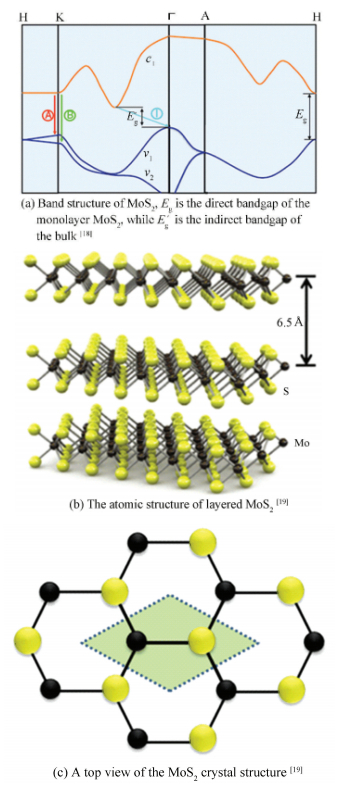 Figure 1 Electronic band and atomic structure of layered MoS2
 At present, monolayer and few-layer MoS2 have been prepared by both "top-down"[20-26] and "bottom-up"[27-38]synthetic strategies (Table 1). The top-down strategies include mechanical cleavage, mechanical force-assisted liquid exfoliation, ion intercalation-assisted liquid exfoliation, and so on. Just like graphene[39-40], 2D MoS2 synthesized by mechanical cleavage is of good quality, however the size of it is pretty small (usually a few micrometers), furthermore, their shape and thickness are not controllable. Using liquid exfoliation to synthesize layered MoS2 makes large-scale production achievable, while its application in electronic devices is hindered by the low quality.
表 1
Micromechanical cleavage top-down [20-22]
Sonication-assisted liquid exfoliation top-down [23-24]
Ion intercalation-assisted liquid exfoliation top-down [25-26]
Chemical vapor deposition bottom-up [27-29]
Molecular beam epitaxy bottom-up [30-31]
Solvothermal synthesis bottom-up [32-33]
Hydrothermal synthesis bottom-up [34-35]
Chemical vapor transport bottom-up [36]
Metal organic chemical vapor deposition bottom-up [37-38]
Table 1 Typical synthetic methods for MoS2
The bottom-up strategies, that is, the direct preparation of 2D materials via chemical reactions from different precursors at certain conditions. The CVD technique is a common bottom-up strategy utilized to synthesize atomically thin nanomaterials on special substrates. Typically, the substrate is put inside of the furnace chamber, and then the gas-phase precursors will react above the substrate to generate ultrathin flakes or films at high temperature. Up to now, it has been successful in growing high-quality single- and few-layered MoS2 on various substrates, including SiO2/Si, sapphire, SrTiO3 and Au. Compared to other bottom-up strategies, the CVD method is most promising in terms of scalability, simple operation and low cost.
However, it is well known that there are so many parameters we should take into account in CVD process like temperature, pressure, flow rate of carrier gas, and so on, which makes it hard for us to control the process of growth. Although many papers and reviews have summarized the synthetic methods of MoS2 and its applications, a systematic review that expounds how these various important factors influence the process of growth is lacking. This work aims to discuss in detail how some parameters such as substrates, kinds of carrier gases and species of Mo precursors affect the quality of the obtained MoS2 by CVD (Fig. 2), which can be also applied to the synthesis of other TMDs.
Figure 2
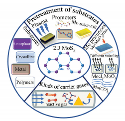 Figure 2 Various important factors influence the CVD process of growing layered MoS2
 2 Influence Factors 2.1 Substrates It is well-known that the CVD routes typically involve a chemical reaction of the precursors, followed by a vapor-solid phase transformation giving rise to the growth of ultrathin MoS2 flakes or films on target substrates[41]. Since different substrates possess different surface structures, various substrates like SiO2/Si, mica, sapphire and Au foil may give diverse growth environments with a wide tunability of domain shape, orientation, as well as size for monolayer MoS2.
2.1.1 SiO2/Si Owing to its well compatibility with Si-based electronics, insulating SiO2/Si is the most prevalent substrate for the preparation of MoS2 by CVD, that means we can fabricate some electron devices like field effect transistor (FET) directly without any transfer process which may have unfavorable effects on the electrical properties of MoS2.
Typically, Najmaei et al.[29] achieved the controlled CVD synthesis of MoS2 atomic layers on SiO2/Si substrate (Fig. 3(a)). They demonstrated that the key point for the synthesis of large-area and high-quality MoS2 films was the uniform nucleation on SiO2 substrates. The Raman results (Fig. 3(c), (d)) shown that MoS2 domains tended to nucleate in the places near to the substrates′ edges, scratches, or rough areas. Based on this phenomenon, they uniformly patterned the substrates with many rectangular SiO2 pillars, directly to create some step edges for nucleation of MoS2 in CVD process (Fig. 3(b)). The as-grown MoS2 films were predominantly monolayer, while a small fraction of which consisted of two or more layers. Because of the isotropy of the amorphous SiO2 surface, the resulting MoS2 films were made up of randomly oriented domains. Finally, they fabricated FET devices to estimate the electrical property of this material by patterning this film via lithography and reactive ion etching. Mobility measurements shown an average of 4.3 ± 0.8 cm2/(V·s), on/off ratios could reach 6×10⁶ (Fig. 3(e), (f)).
Figure 3
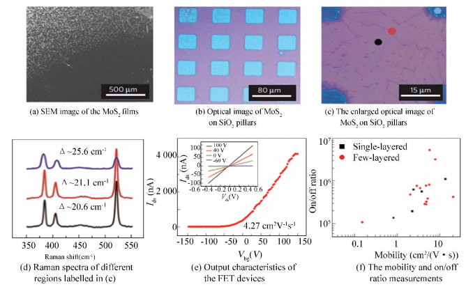 Figure 3 Optical and electrical characterization of the obtained MoS2 on SiO2/Si substrate[29]
 2.1.2 Mica Other than SiO2/Si substrate, other insulating materials such as mica, sapphire, SrTiO3 and LaAlO3 were also used for synthesizing the monolayer MoS2 by CVD. Noteworthily, their atomically smooth crystalline surfaces, as well as different interfacial energetics, and possible lattice-match to MoS2, could also lead to additional controllable orientation and morphology of MoS2 by van der Waals (vdW) epitaxy.
Fluorophlogopite mica (KMg3AlSi3O10F2) is regarded as an ideal vdW epitaxy substrate due to its surface inertness, atomic flatness, as well as the ordered hexagonal lattice structure. These unique features endow mica as a superior material for epitaxially growing layered materials which possess the same crystal symmetry. Particularly, the lattice symmetry of mica is in agreement with that of MoS2 and there is small lattice mismatch (~2.7%) between mica and MoS2, which could be used for growing monolayer MoS2 on mica via the vdW epitaxy.
Using low-pressure chemical vapor deposition (LPCVD), Ji et al.[42] successfully synthesized MoS2 monolayer on a mica substrate (Fig. 4(a)). As shown in SEM (Fig. 4(b)), the initial grown MoS2 were triangular flakes, exhibiting almost the same size and orientation, as labelled by the dashed yellow rhombus. With the increasing of the growth time, the MoS2 domain enlarged in size to generate larger flakes and even centimeter-scale, monolayer MoS2 films (Fig. 4(c), (d)). Another interesting finding was that the MoS2 domains on mica preferred to merge together via in-plane stitching, rather than overlap with each other. Thus, this growth system was identified to be dominated by a vdW epitaxial mechanism.
Figure 4
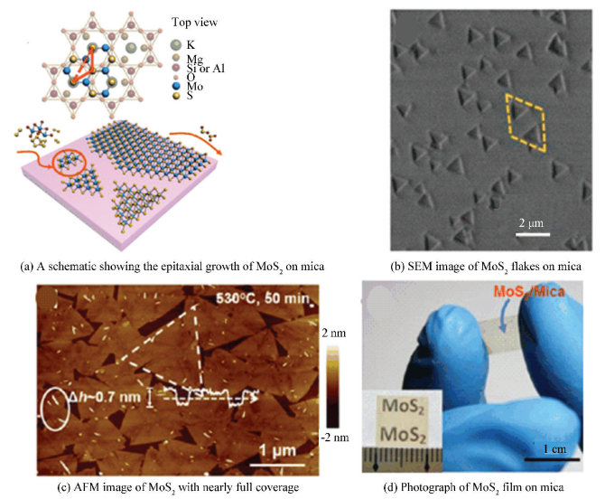 Figure 4 LPCVD synthesis of monolayer MoS2 flakes on mica[42]
 2.1.3 Sapphire Additionally, sapphire (0001) is also an ideal substrate frequently used for the epitaxial growth of a large amount of crystals due to its atomically flat surface and possible lattice-matching with the target materials. In addition, it must be mentioned that monolayer MoS2 grown on sapphire may have higher quality than those on SiO2/Si substrates owing to the large-scale thickness uniformity and low content of oxygen doping.
Similarly, Ji et al.[43] controllably synthesized high-quality monolayer MoS2 flakes and films on sapphire (0001) substrates by using LPCVD (Fig. 5(a)). With growth time increasing, triangular MoS2 domains of different orientation grew up gradually and began to coalesce with each other (Fig. 5(b)), finally resulting a uniform thickness, high crystal quality but polycrystalline monolayer MoS2 (Fig. 5(c)). This phenomenon revealed that perfect epitaxial characteristics of MoS2 on sapphire were almost totally absent. Based on density functional theory (DFT), this growth behavior was thought to result from the small differences of the interfacial binding energy between sapphire and MoS2 at diverse relative rotations.
Figure 5
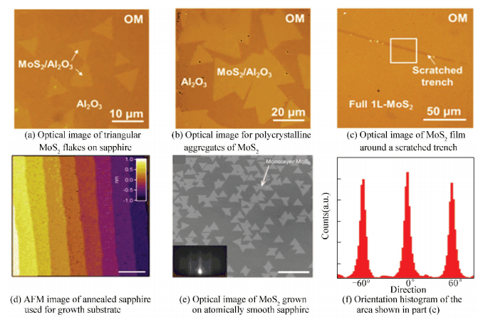 Figure 5 Monolayer MoS2 grown on sapphire substrates[44]
 In order to decrease the grain boundaries which were unfavorable for the mechanical and electrical performance of the MoS2, Dumcenco et al.[44] used EPI-ready grade sapphire substrates to regulate the crystal orientation of MoS2 domains during CVD process, thus these highly aligned domains could merge into a uniform layer with a decreased amount of grain boundaries. The key to better aligning of individual MoS2 flakes was preparing atomically smooth terraces on the surface of sapphire (Fig. 5(d)) by annealing it at 1 000 ℃ for 1 h before the growth process. A careful orientation examination disclosed that the most of single-crystal MoS2 flakes (91.5% displayed in Fig. 5(e)) were well aligned with edge orientations as multiples of 60° (Fig. 5(f)). Only a small part of the MoS2 flakes (6%) possessed an angle of ±30°, while the rest (2.5%) displayed other orientations. Undoubtedly, such highly aligned MoS2 domains sharply decreased the number of tilted grain boundaries.
2.1.4 SrTiO3 and LaAlO3 Recently, some novel single-crystal substrates were also reported to be capable of mediating the diffusion pathways of precursor species, which provided additional chances for us to engineer the morphology of MoS2.
For example, Zhang et al.[45] reported a controllable preparation of dendritic monolayer MoS2 on SrTiO3 (STO (001)) substrate using LPCVD. The obtained MoS2 flakes (Fig. 6(a)) or films (Fig. 6(c)) possessed the unique feature of strictly monolayer, coverage adjustable from sub-monolayer to complete monolayer (Fig. 6(b)), and flake shape tunable from fractal to compact by changing the conditions of growth. This phenomenon could be explained by a diffusion-limited aggregation mechanism. The unique dendritic structure of MoS2 with abundant edges which were considered to be the active sites for hydrogen evolution reaction (HER) made it a promising catalyst for practical applications.
Figure 6
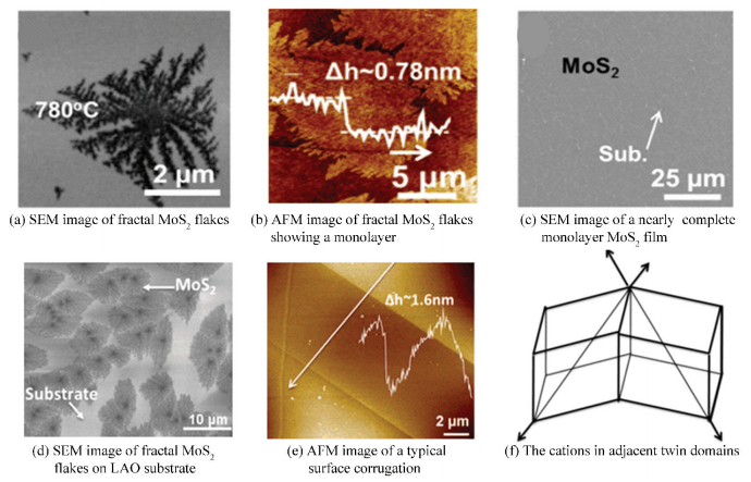 Figure 6 LPCVD synthesis of monolayer MoS2 on STO and LAO substrates[46]
 Afterwards, Li et al.[46]also controllably synthesized the dendritic MoS2 (Fig. 6(d)) on a novel single-crystal LaAlO3 (LAO (100)) substrate through LPCVD. It was found that the LAO substrates commonly twinned and generated a triangular surface corrugation (Fig. 6(e), (f)), which could be ascribed to a phase transformation between the high-temperature cubic prototype phase and rhombohedral lattice below critical temperature. Therefore, the domain wall would divide the corrugation into two parts, isolating the steps from one part to another. Thus, there were steps on the one side, however the other side of the domain wall owned more smooth surface, even if both two parts were (100) lattice planes. The atomic steps on one side supplied plenty of nucleation sites, giving rise to lots of nuclei located along the steps, which leaded to the growth of fractal MoS2 flakes with a mass of active edge sites, exhibiting a promising HER performance.
Briefly, although SiO2/Si is the prevailing substrate for synthesizing high-quality layered MoS2 currently by CVD, a lot of recent literature demonstrates that the amorphous surface of SiO2 is not effective in catching the MoO3-x species and controlling the crystallographic orientation for growing large-area, thickness uniform and single-crystal MoS2 films. On the country, insulating single-crystal substrates are more reasonable for the growth of layered MoS2, creating more opportunities for us to engineer the domain orientation, micro-morphology, merging behavior and growth mechanism.
2.1.5 Au foil Recently, synthesizing layered MoS2 on Au foil emerges as a fascinating growth system owing to its direct application in HER without a complex transfer process which will lead some quality degradation, on the other hand, directly growing MoS2 on Au substrates is convenient for the further characterizations by scanning tunneling microscopy and spectroscopy (STM/STS), which can reveal some fundamental characteristices of the monolayer MoS2.
For example, Shi et al.[47] developed the controllable synthesis of domain size tunable monolayer MoS2 flakes (Fig. 7(a), (b)) on Au foils by LPCVD. Interestingly, on the basis of Raman spectra of MoS2 flakes grown under different source-substrate distance (Dss) and temperature, they concluded that the MoS2 flakes grown on Au foil were strictly monolayer regardless of growth temperature and Dss, which indicated that the growth traits of MoS2 on Au foil resulted from the strong interaction between Au foil and MoS2. This phenomenon was in great contrast with that of MoS2 on some insulating substrates like SiO2/Si and sapphire, having some possibility to form few-layer MoS2.
Figure 7
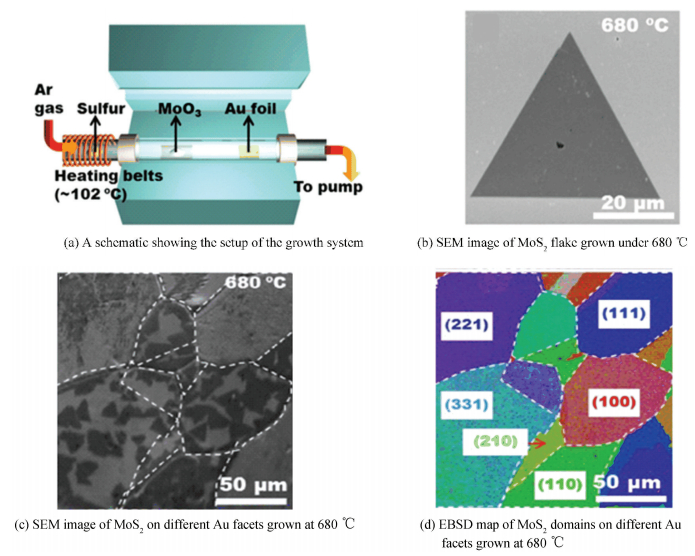 Figure 7 LPCVD synthesis of monolayer MoS2 flakes on Au foils[47]
 Another unanticipated finding was that the crystallography of Au substrate had a dramatic impact on the growth process[48], where MoS2 domains were more likely to generate on Au (110) and Au (100) facets than Au (111) at high temperatures (Fig. 7(c), (d)).Obviously, Au foil has many advantages when it comes to synthesize high-quality monolayer MoS2, however high cost of which may hinder its future application. Thus, hunting for other stable metals or alloys is also vital for lowering the costs of production and achieving their practical applications.
2.1.6 Polyimide Besides insulating and metal substrates, polymers can also be utilized as target substrates for the synthesis of large-domain and high-quality monolayer MoS2. Directly growing 2D materials on flexible materials provides a good idea to combine the scalable synthesis technique with the target flexible substrates, taking a crucial step toward practical fabrication of flexible functional films. However, the high-temperature synthetic condition (>600 ℃) for MoS2 by CVD are not suitable for polymers, which usually have relatively low thermal stability[49].
What's exciting is that Gong et al.[50] directly grew monolayer single-crystal MoS2 flakes on polyimide (PI) substrates by a simple CVD method using ammonium molybdate ((NH4)2MoO4) as a Mo precursor rather than traditionally used molybdenum trioxide (MoO3) at 450 ℃(Fig. 8(a), (b)), at which temperature PI was still stable and flexible (Fig. 8(c), (d)). Moreover, the MoO3 derived from the decomposition of (NH4)2MoO4 was more active than the commercial MoO3 powder and the gaseous products accompanied with the decomposition process could bring out the MoO3 molecules, making the reaction kinetically more favored.
Figure 8
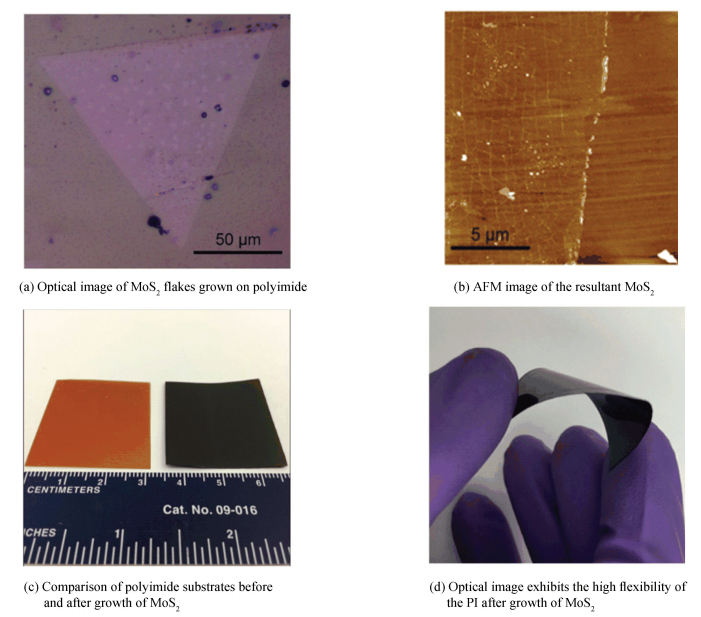 Figure 8 Growth of monolayer MoS2 on PI substrate[50]
 As discussed above, we can be clearly aware that the substrates play a significant role in the synthesis and application of atomically thin MoS2. Notably, various substrates possess diverse surface structures and interfacial binding strengths, that means during growth, the interaction between the gaseous precursors and the substrates is different, which leads to different densities of MoS2 nuclei at the initial period of the growth. In addition, distinct crystalline states of the substrates determine the orientation of MoS2 domains, if the surface of the substrate is amorphous, the MoS2 domains may display randomly on the substrates, however, while the substrate possesses atomically smooth crystalline surface and small lattice mismatch with MoS2, the epitaxial domains may align at one direction. Upon different domains merging together, there will be no grain boundaries generated, which would be detrimental to the electrical and mechanical performance of the MoS2. From the perspective of application, how to choose a proper growth substrate is also important. Even though amorphous surface of SiO2 is not effective in capturing the MoO3-x species and controlling the crystallographic orientation, SiO2/Si is still the prevailing substrate for synthesizing layered MoS2 currently by CVD owing to its high compatibility with Si-based electronics. Moreover, if we want to apply it in the area of electrocatalysis, we would better choose some substrates with high conductivity like Au or carbon paper. However, if we want to combine 2D materials with flexible films, polymers substrates should be our choices.
Up to now, so many kinds of substrates have been utilized in the growth of MoS2 such as SiO2/Si, mica, sapphire, STO, Au foils and PI. Briefly, every substrate has its own advantages and disadvantages, different substrates may give diverse growth mechanism with a wide tunability of domain shape, orientation and size for monolayer MoS2, and the final decision of the substrate may depend on the further application of the obtained MoS2 flakes or films.
2.2 Pretreatment of the Substrates It is generally accepted that the formation process of MoS2 domains mainly contains two steps: nucleation and growth. Achieving a proper concentration of nuclei is very vital to synthesize high quality layered MoS2. Pretreating the surface of substrates before growth is one of the novel strategies to create some nucleation sites artificially or change the state of the surface of the substrates for enhancing the interaction between the precursors and the substrates, which will promote the nucleation of MoS2.
2.2.1 Seeding aromatic molecules on surfaces For the first time, Lee et al.[51] obtained highly crystalline and large-area MoS2 layers on amorphous SiO2/Si substrate using graphene-like molecules like reduced graphene oxide (rGO), perylene-3, 4, 9, 10-tetracarboxylic acid tetrapotassium salt (PTAS) and perylene-3, 4, 9, 10-tetracarboxylic dianhydride (PTCDA) as the seeds for growing. However, the authors did not get the strict monolayer MoS2 and further discussed the effect of the graphene-like molecules in detail. Lately, Kong et al.[52] synthesized high-quality uniform single crystalline structure MoS2 monolayers using APCVD with the seeding of PTAS (Fig. 9(a)), which was stable at high temperature compared to other aromatic molecules (Fig. 9(b)). In addition, PTAS had a high solubility in water, making the PTAS molecules distributed uniform on the surface of substrates. After seeding the substrate with PTAS, monolayer MoS2 flakes (Fig. 9(c)) can grow successfully on the substrates. As a comparison, they can only observe MoS2 particles on the bare substrate without the seeds. Thus, the existence of PTAS was able to adsorb the precursor molecules and promote the initiation of heterogeneous nucleation, significantly enabling layer growth. As a conclusion, they disclosed that seeding the substrates with an appropriate aromatic molecule having a high thermal stability and better solubility in solvent was crucial for the synthesis of high-quality MoS2 monolayers.
Figure 9
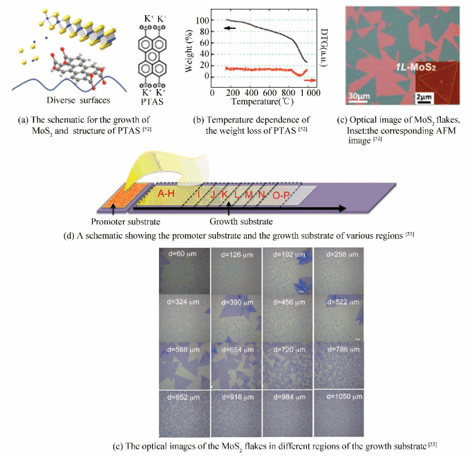 Figure 9 Growth of layered MoS2 by seeding aromatic molecules on the surface of substrates
 To further explore this concept, they systematically investigated the effect of the seeding promoter in preparing monolayer MoS2[53]. Owing to different distance between the promoter substrate and various regions of growth substrate, the different growth regions might have disparate concentration of seeds (Fig. 9(d)). By analyzing the growth results of different growth regions (Fig. 9(e)), they indicated that a proper concentration of the promoters was of great importance to facilitate the nucleation of MoS2 on the SiO2/Si substrate. Furthermore, except for the already found seeding promoters like PTAS, twelve kinds of other aromatic molecules such as copper phthalocyanine (CuPc), PTCDA, copper (Ⅱ) 1, 2, 3, 4, 8, 9, 10, 11, 15, 16, 17, 18, 22, 23, 24, 25-hexadecafluoro-29H, 31H-phthalocyanine (F16CuPc) were further used as promoters for the growth of MoS2, and many of them were discovered to be effective. However, when some inorganic nanoparticles were utilized as promoters, they found no enhancement for the synthesis of monolayer MoS2. Moreover, since PTAS was a salt and had a high solubility in water, it can only work normally on hydrophilic substrates. However, the above newfound aromatic molecules can be uniformly and easily deposited on various substrates by thermal evaporation, hence promoting the synthesis of MoS2 on various hydrophobic substrates, such as graphene, gold, and h-BN. It is anticipated that these studies will provide more understanding on the mechanism of seed-enhanced growth.
2.2.2 Plasma treatment Pretreating the substrate with plasma is a fresh approach to facilitate uniform nucleation and layer growth of MoS2. Jeon et al.[54] reported that large-area, varied numbers of MoS2 layers can be obtained by pretreating SiO2/Si substrates with the oxygen plasma (Fig. 10(a)). The XPS characterization shown that the chemical structure of the SiO2/Si surface had changed after oxygen plasma treatment. More specifically, with the time of treatment increasing, the Si 2p and O 1s peaks shifted to higher binding energies, corresponding to Si-(O or OH)4 bonding, which resulted in a higher surface reactivity and a better lattice matching with hexagonal MoS2. Compared to the original SiO2/Si substrate, the surface of those pretreated with oxygen plasma became more hydrophilic, thus decreasing the surface energy and facilitating uniform nucleation and layer growth of MoS2. Another interesting finding was that they can controllably synthesize monolayer, bilayer and trilayer MoS2 films by simply adjusting the duration (90 s, 120 s and 300 s) of the plasma treatment on the SiO2/Si, which can be proved by AFM characterization (Fig. 10(b), (c), (d)). This interesting phenomenon indicated that the growth process of these layer-controlled MoS2 film was self-limiting, which can be explained by the interaction between MoS2 and substrates which changed due to the plasma treatment time.
Figure 10
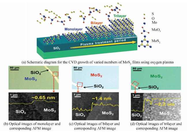 Figure 10 Growth of varied numbers of layered MoS2 by pretreating SiO2/Si with the oxygen plasma[54]
 2.2.3 Pre-deposited Au film Atomic Mo film can serve as a Mo precursor to synthesize atomic MoS2 layers, and the thickness of the MoS2 layer is only dependent on the thickness of pre-deposited Mo film. However, the preparation of large-area atomically thin Mo film on the substrate is a difficult problem to overcome at the present. Notably, Song et al.[55] have developed a fancy method to prepare atomically thin MoS2 layers in expected sizes and patterns via Au-assisted CVD. Firstly, they pre-deposited 50 nm Au thin film on a Si substrate (Fig. 11(a)), and then it would react with [Mo(CO)6] to form the Mo-Au alloy on the surface of Au film, which was able to act as an excellent Mo reservoir. When the H2S introduced into the chamber at 300 ℃ afterwards, the surface Mo-Au alloy would react with it and the buried Mo atom diffused out, then forming atomically thin MoS2 layers (Fig. 11(e)). Therefore, the formation of the surface Mo-Au alloy was supposed to be the key role in realization of uniform MoS2 atomic layers (Fig. 11(b), (c), (d)). In this sense, we can achieve patterned growth of MoS2 atomic layers simply by designing the pattern of the pre-deposited Au film. This was the first time to present the growth of atomically thin MoS2 in a desired pattern without any pretreatment.
Figure 11
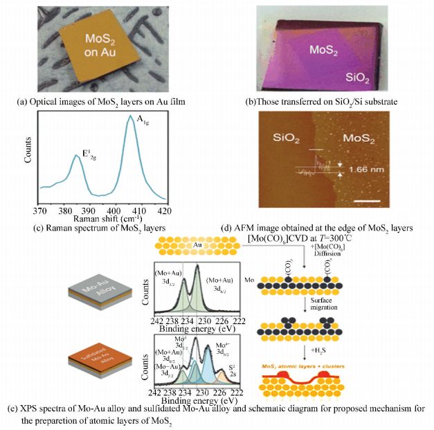 Figure 11 Synthesis of atomically thin MoS2 layers in expected sizes and patterns via Au-assisted CVD[55]
 Directly growing 2D semiconductor materials on SiO2/Si substrate is of great important to its potential application in the field of electron devices. However, as mentioned above, the interaction between the amorphous surface of SiO2/Si substrate and gaseous Mo precursors is pretty weak, resulting the initial nucleation process being rather difficult. In order to solve this problem, researchers try to pretreat the substrate before the growth process, specifically including seeding the substrate with some aromatic molecule like PTAS to adsorb the precursor molecules and promote the initiation of heterogeneous nucleation, pretreating the substrate with plasma to decrease the surface energy and facilitate uniform nucleation, depositing Au thin film on the SiO2/Si substrate to form Mo-Au alloy which could act as an excellent Mo reservoir during the growth, and so on. In general, artificially modifying the SiO2/Si substrate and activating the inert state of the surface are the key points to enhance the interaction between the SiO2/Si substrate and the Mo precursors, thus promoting the initial nucleation of MoS2.
2.3 Kinds of Carrier Gases As we all know, the carrier gases play an important role in the growth of MoS2, whose effects can be divided into two parts. Apparently, the flow rates of the carrier gases determine the amount of the precursors brought to the substrates per unit time, which will influence the growth kinetics of layered MoS2. Furthermore, the recipe of the carrier gases is also vital for the growth of MoS2, which is usually proceeded under inert gas like high purity argon or nitrogen. However, if some reactive gas like O2 or H2 is included, the growth process will be greatly influenced[56-58].
2.3.1 O2 Recently, Chen et al.[56]developed a novel oxygen-assisted chemical vapor deposition (OACVD) strategy to synthesize high-quality monolayer MoS2. Fig. 12(a)-(c) shown the optical images of MoS2 grown on sapphire substrates with the O2 flow rate ranging from 0 to 2 sccm. According to the AFM image in the inset of Fig. 12(a), a great many MoS2 particles were observed on both the MoS2 and substrate without O2. By contrast, a clean monolayer MoS2 film was obtained with just 1 sccm O2 brought into the chamber (Fig. 12(b)), which was also consistent with the observation from the AFM image of Fig. 12(b). With increasing the O2 flow rate to 2 sccm, the length of triangular MoS2 flakes could reach about 350 μm (Fig. 12(c)). It was interesting to find that the maximum domain size of the obtained MoS2 decreased gradually with the O2 flow rate increased from 3 to 5 sccm (Fig. 12(d)-(f)). To gain a better understanding of this phenomenon, the authors plotted the average length (l) of the MoS2 flakes grown under 2 sccm O2 as a function of growth duration (Fig. 12(g)). Typically, after growing for 10, 20, and 30 min, maximum domain size of MoS2 could reach 125, 275, and 350 μm, respectively. However, when further increasing the growth time, the as-grown domains would be etched little by little. Finally, the as-grown MoS2 domains would completely disappear after 60 min of growth.
Figure 12
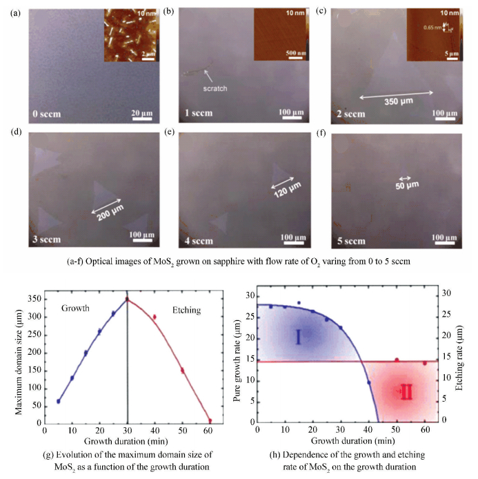 Figure 12 Growth of monolayer MoS2 large domains and films at variable oxygen flow rates and growth durations[56]
 Their findings suggest that a small amount of O2 could decrease nucleation density of MoS2 by smearing out some unsteady nuclei and chemically oxidizing its edges, resulting in the Mo and S atoms becoming MoO3 and SO2 gas to decompose. Hence, they concluded that the process of growth was accompanied by the etching effect of O2. To gain more insight, the relationship between the growth, etching rates of MoS2 and growth duration was illuminated in Fig. 12(h). The blue curves indicated that, in the initial period, the growth rate was almost stable, and then it gradually decreased as the time went on. While the rate of etching was supposed to be fixed, it just depended on the flow rate of O2. Hence, only when the growth rate was higher than that of etching, the growth was proceeding. Upon the increasing of the growth duration further, the rate of etching would be higher than the growth, resulting the MoS2 domains shrinking rapidly.
Using this OACVD method, this group recently synthesized wafer-scale highly aligned uniform and continuous monolayer MoS2 films by epitaxial growth on sapphire wafer[57]. They illustrated that the formation of MoS2 on sapphire substrate coincides with the classic surface-limited growth mechanism. More specifically, the energy barrier of absorption on MoS2 flakes was larger than that on a sapphire substrate. In this case, the arriving precursors would quickly migrate to the edge of MoS2 forming large film or be etched by O2. Except for the etching effect, the existence of O2 could prevent the MoO3 from sulfidation and guarantee its incessant evaporation in the growth process. During the experiment, they did not find any obvious change of MoO3 before and after the growth, as shown in Fig. 13(b) and (d). As a comparison, the MoO3 would react with S vapor to form MoS2 and MoO2 (Fig. 13(a), (c)) without the introduction of O2. It was commonly known that the melting point of MoS2 was higher than that of MoO3, thus the evaporation would stop at that temperature when the MoO3 was sulfured, which was a typical poisoning effect we avoided by introducing small amounts of O2. With the assistance of O2, the MoO3 was protected and could evaporate continuously enabling us to effectively synthesize very large domain sizes and even obtain wafer scale uniform MoS2 films (Fig. 13(e)).
Figure 13
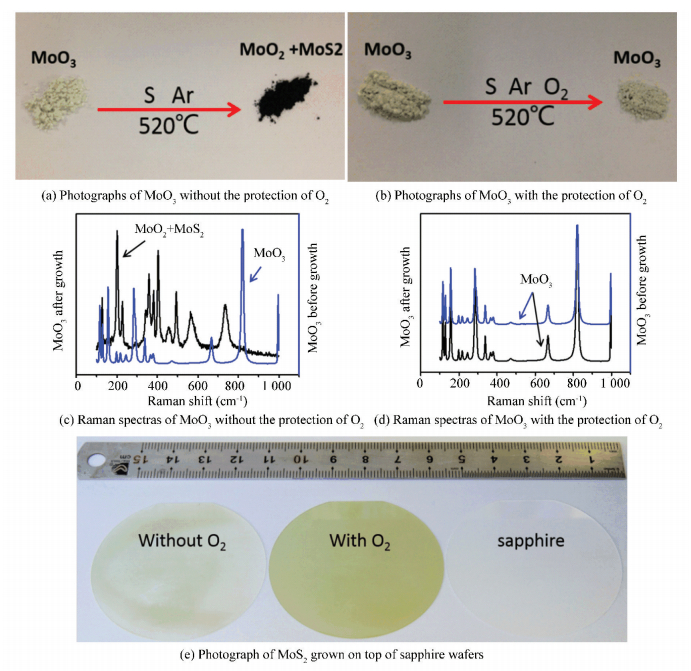 Figure 13 Growth of monolayer MoS2 on the sapphire wafer[57]
 2.3.2 H2 As the same with O2, H2 also has a double action in the growth of MoS2. Shi et al.[58] successfully prepared monolayer MoS2 flakes on Au substrates and systematically explored the effect of H2 via LPCVD. SEM images in Fig. 14(a) and (b) shown that when the H2 flow rate changing from 0 to 3 sccm, the length of MoS2 flakes would increase from 7.8 to 20.9 μm. With the flow rate of H2 increasing further to 5 and 6 sccm, the average length could reach about 47.8 and 55.8 μm (Fig. 14(c), (d)), respectively. However, while further increasing the H2 flow rate to 8 and 10 sccm, the edge lengths of grown MoS2 domains began to decrease to 13.5 and 7.3 μm (Fig. 14(e), (f)).
Figure 14
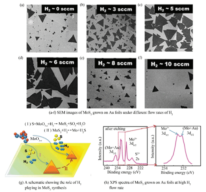 Figure 14 Growth of monolayer MoS2 flakes at variable H2 flow rate[58]
 In order to shed light on the interesting experimental results, the role of H2 was playing in the CVD process should be analyzed in detail. On one hand, H2 could provide a reductive atmosphere which might be favorable for the efficient sulfurization of MoO3 and the fast formation of MoS2 at low H2 flow rate (the involved chemical reaction was shown in Eq.(Ⅰ) of Fig. 14(g)). In addition, a small amount of H2 was also able to reduce the nucleation density of MoS2 by removing some impurities on Au substrates since the impurities could serve as nucleation sites for the growth of MoS2. On the other hand, as the flow rate of H2 becoming higher, MoO3 source would be reduced to Mo metals and this might directly prevent the Mo precursor from suppling and then stop the subsequent growth of MoS2. Furthermore, a high flow rate of H2 would also etch the existing MoS2 domains, as shown in Eq.(Ⅱ) of Fig. 14(g). From the XPS results (Fig. 14(h)), we observed that the Mo metal (etching product) can form Mo-Au alloys with the Au films at high temperature. Therefore, the reduced MoO3 precursor supply and etching effect would work together to decrease domain size of MoS2 at high H2 flow rate. In this sense, we can achieve large-size MoS2 flakes on Au foils by simply controlling an appropriate flow rate of H2.
Based on the above experiment details, we can infer that the growth results are very sensitive to the ambient atmospheres. Only a small change about the amount of reactive gas like O2 or H2, results in the quality of the obtained MoS2 having a big difference. Generally, these active gases often have a double action to the growth of MoS2, even though their specific effect are different. When the amount of reactive gas is small, it will help to synthesize large-size MoS2 flakes or films via reducing the nucleation density of MoS2. Upon increasing the amount of reactive gas, it will etch the existing MoS2 domains predominantly, resulting a small-size MoS2 domain. Bearing this in mind, we can easily achieve high-quality MoS2 monolayer with a controllable size by adjusting the amount of reactive gas or reaction time.
2.4 Species of Mo Precursors Hitherto, there are so many different kinds of Mo precursors employed for the growth of atomically thin MoS2 including Mo film, MoO2, MoO3, MoCl5, (NH4)2MoS4, Mo(CO)6, and so on. Since different Mo precursors have various physical and chemical properties, the concrete parameters used in the experiments may differ greatly. In addition, the thickness and size of MoS2 flakes or films obtained by diverse Mo precursors may also vary from each other.
2.4.1 Mo film Generally, Mo foil might be one of the earliest Mo precursors used to synthesize atomically thin MoS2[28, 59-61]. Zhan et al.[28] demonstrated a direct synthesis of single- and few layered MoS2 by APCVD using a pre-deposition of Mo film as Mo precursor on SiO2 substrates followed by sulphurization. Specifically, a thin Mo layer (approximately 1-5 nm) was pre-deposited on SiO2 substrate by an e-beam evaporator firstly, and then sulfur vapor was brought in and reacted with Mo film to form atomically thin MoS2 film at 750 ℃. It was interesting to find that the thickness and size of the MoS2 layer were only dependent on the thickness of pre-deposited Mo film and the size of the SiO2 substrate, indicating that the synthetic process was controllable and scalable, that is, films of any size and thickness can be prepared with good uniformity, which made it a potential candidate to meet the demands from future applications. However, they cannot get strict monolayer and single-crystal MoS2 via this method of directly sulfurating the thin Mo film.
Recently, Li et al.[61] developed a facile and environmentally friendly strategy to synthesize monolayer and few-layer MoS2 single crystals by a simple one-step rapid sulfurization of Mo film. In this growth system, they designed a special reactor with a confined space to suppress the sublimation of sulfur and increase the probability of nucleation for synthesizing MoS2 under an sufficient sulfur atmosphere (Fig. 15(a)). For Reactor 1, the Mo film coated with S plate was placed in the gap between two bare SiO2/Si substrates. Fig. 15(b) shown the optical images of MoS2 flakes obtained by Reactor 1. More importantly, most of the as-grown MoS2 flakes were strictly monolayers, which can be proved by AFM characterization. As for Reactor 2, a single S plate was sandwiched between two SiO2/Si substrates coated with Mo films. Fig. 15(c) displayed the optical images of monolayer and few-layer MoS2 flakes synthesized by Reactor 2, the thickness of which can be confirmed easily by optical contrast. Therefore, simply by changing the reactor design, they can controllably obtain monolayer and few-layer MoS2 flakes. In order to illuminate the important effects of the space-confined design, as a comparison, the top SiO2/Si substrate in Reactor 1 was removed and then annealed under the same conditions. While the experiment results shown that no monolayer MoS2 single crystals were obtained, which can be explained by the rapid sulfur evaporation and the reduced probability of nucleation for synthesizing MoS2 single crystals. As far as I known, this is the first time to achieve monolayer MoS2 single crystals by direct sulfurization of Mo foil. In addition, only very small amounts of precursors (Mo~3 μg, S~50 mg) were needed in this synthesis, far less than those used in conventional CVD approaches.
Figure 15
 Figure 15 Growth of monolayer and few-layer MoS2 flakes by a one-step rapid sulfurization of Mo film[61]
 2.4.2 MoO3 In a general way, the sulphurization of MoO3 has been one of the most prevalent approaches for the synthesis of atomically thin MoS2. So far, majority of growing MoS2 monolayers through CVD processes involved the utilization of MoO3 powder as a Mo precursor. Lee et al.[51]firstly demonstrated that MoO3 is an appropriate precursor for controllable synthesis of MoS2 thin films. They systematically investigated the nucleation and growth of layered MoS2 in CVD process assisted by some graphene-like species, the effect of which has been discussed above. In this sense, we can directly obtain large-size MoS2 monolayer on amorphous SiO2 substrate without using highly crystalline substrates or rigorous ultrahigh vacuum. During this synthesis of MoS2, the furnace was heated to 650 ℃ in a N2 environment, at which temperature MoO3 powder would be reduced by the sulfur to produce volatile suboxide MoO3-x. These compounds would diffuse quickly to the substrate and react further with sulfur vapor to form highly crystalline MoS2 films, whose size can be up to several millimeters. Furthermore, some characterizations such as Raman, PL, AFM all suggested that the obtained layered MoS2 films contained monolayer, bilayer and few-layer.
Inspired by using the thin Mo film as Mo precursor to synthesize atomic-layered MoS2, Lin et al.[62]presented that wafer-scale MoS2 atomic thin layers can be achieved by a simple and scalable two-step annealing process to transform MoO3 layers into MoS2 layers. Firstly, a thin layer of MoO3 (approximately 3.6 nm) was pre-deposited on a bare sapphire substrate via thermal evaporation, and then the coated MoO3 was reduced to MoO2 or other suboxides at 500 ℃ for 1 h in Ar/H2 atmosphere during the first annealing process. In the second thermal process, the sample was annealed at 600 Torr and 1 000 ℃ for 30 min in a sulfur-rich environment. Further HRTEM, Raman, PL and AFM characterizations shown that these obtained films were polycrystalline and uniform few-layer. In addition, these MoS2 films were thickness controllable and can be easily transferred to other substrates, making these films favorable for flexible electronic and optoelectronic devices.
Instead of using solid MoO3 powder as a Mo precursor, Lee et al.[63]developed a novel and simple way for using a low concentration of MoO3 solution as Mo precursor to lead a relatively low supersaturation state of the vapor reactants, resulting in a reduced nucleation density, which was vital for growth of large domain size MoS2. Adopting this proposal, a thin precursor film containing a small amount of MoO3 (≈0.01 mg) was prepared on SiO2/Si as a source substrate (Fig. 16(a), (b)), which can decrease nucleation density to 32 nuclei mm-2 over the whole substrate surface at a high temperature of 800 ℃. Due to the relative low nucleation density and proper growth rate, a highly crystalline and centimeter-scale MoS2 monolayer can be grown directly on the target substrate, and a large size (500 μm) MoS2 single crystals can be observed in the edge of the substrate (Fig. 16(c), (d), (e)). In addition to this, they discovered that the monolayer MoS2 possessed an outstanding optical property with a relative small full-width-half-maximum (FWHM) of 48 meV (Fig. 16(f)), which was comparable to or even better than that of exfoliated single-crystal MoS2 monolayers.
Figure 16
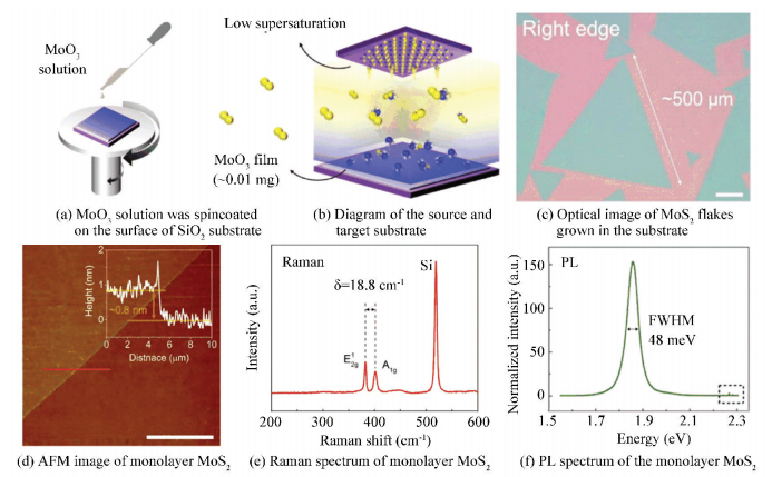 Figure 16 Synthesis of monolayer MoS2 film by solution-processed precursor deposition[63]
 2.4.3 MoO2 As an another kind of molybdenum oxide, MoO2 can also be applied to prepare highly crystalline MoS2. For example, Wang et al.[64] reported a fresh method for synthesis of rhombohedral MoS2 flakes via sulfurizing of MoO2 nanoplates (Fig. 17(a)). In the first step, evaporated MoO3 reacted with S at 650-850 ℃ to form the MoO2 nanoplates on SiO2/Si substrate, and then the MoO2 templates were secondary annealed at 850-950 ℃ for 0.5-6 h in a sulfur atmosphere. During this process, varied numbers of MoO2 layers can be sulfurized to MoS2 depending on the annealing time (Fig. 17(b)). As shown in Raman mapping (Fig. 17(c), (d), (e)), the obtained MoS2 flakes were remarkably uniform and possess a domain size of ~10 μm. Because of high quality of the MoS2 flakes, the carrier mobilities and on/off current ratio of back-gated FETs fabricated by the obtained MoS2 was comparable to that of prepared by mechanical cleavage. This novel strategy paves a new way for synthesis of highly crystalline MoS2 with controlled number of layers, making this material a promising material for various future applications.
Figure 17
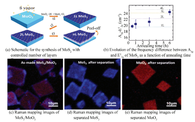 Figure 17 Synthesis of MoS2 flakes with controlled shape and number of layers[64]
 2.4.4 MoCl5 As we discussed in Section 2.3.1, MoO3 powders will be poisoned during the process of sulfurization and cannot evaporate incessantly to effectively grow large domain MoS2. Furthermore, toxic and corrosive SO2 gas will be generated during the sulfurization of MoO3. Compared with MoO3, MoCl5 has a lower sublimation temperature, thus it cannot be sulfurized and poisoned before migrating to the high temperature growth zone.
Using MoCl5 as Mo precursor, Yu et al.[65]developed a controllable strategy to prepare high-quality monolayer and few-layer MoS2 films with great uniformity. Typically, the MoCl5 and sulfur vapor can react to form MoS2 species at elevated temperature, which might deposit onto the receiving substrates to produce MoS2 films subsequently. It should be pointed out that the number of the obtained MoS2 layers can be accurately modulated through changing the dosage of MoCl5 precursor used in experiments (Table 2). In addition, they had also successfully synthesized uniform MoS2 films on diverse substrates including SiO2/Si, sapphire and graphite. It was important to highlight that this synthetic method can be scaled up for the applications of electronics and optoelectronics.
表 2
< 1 No deposition N/A
1-4 1 layer 20.2-21.2
5-15 2 layer 22.4-23.2
15-25 3 layer 23.6-23.9
25-35 4 layer 24.0-24.2
Table 2 Correlation of the amount of MoCl5 and the layer number of MoS2 films[65]
2.4.5 (NH4)2MoS4 Pyrolysis of the precursor containing Mo and S is also a good idea to synthesize layered MoS2. As a typical example, Liu et al.[66] developed a two-step decomposition of (NH4)2MoS4 to synthesize highly crystalline MoS2 thin film on insulating substrates (Fig. 18(a)). After the first thermal process under 500 ℃ for 1 h, the crystal structure of the obtained MoS2 was not very good, and then the sample was placed into the furnace chamber for annealing to improve the quality of MoS2 in an atmosphere of sulfur vapor. Notably, the introduction of sulfur during the second annealing observably improved the quality of MoS2 film (Fig. 18(b), (c), (d)). Furthermore, these MoS2 thin films on the growth substrate can be transferred with ease to other substrates. It was noteworthy that the bottom gate FET made by these MoS2 thin layers displayed n-type behaviors with carrier mobility up to 6 cm2/(V·s) and the on/off current ratio ~105, which was comparable with the FET devices fabricated by the mechanically exfoliated MoS2.
Figure 18
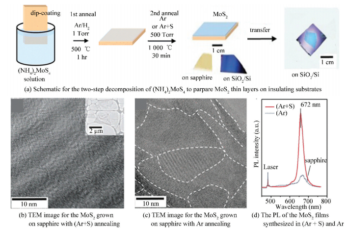 Figure 18 Two-step decomposition of (NH4)2MoS4 for the synthesis of MoS2 thin films[66]
 2.4.6 Mo(CO)6 Beyond solid and liquid Mo precursor, Mo(CO)6 can be a special gaseous Mo precursor for the controllable growth of MoS2. Recently, Kumar et al.[67] demonstrated a simple CVD strategy using Mo(CO)6 and H2S as precursors (Fig. 19(a)), which could achieve synthesis of uniform n-layered (n = 1, 2, 3, … >6) MoS2 films (Fig. 19(d)) on a variety of substrates, including SiO2/Si, sapphire and fused quartz. In this growth system, the low boiling point of Mo(CO)6 (~156 ℃) and H2S made these ideal precursors for the growth of MoS2 by CVD. It should be pointed out that all precursors (Mo(CO)6 and H2S) were introduced into the reaction chamber in the form of vapor phase, in which case we can easily control the concentration of the precursors and then reduce nucleation to form large domain and high quality MoS2. The layered MoS2 grown on the substrates has been researched by AFM (Fig. 19(c)) and Raman (Fig. 19(e)) to confirm the number of layers, their crystallinity and uniformity. In addition, through SEM characterization (Fig. 19(b)), they found that the edge length of monolayer single-crystalline MoS2 flakes grown under relatively low pressure can reach as large as 25 μm. Because of the Mo vacancy, the as-prepared MoS2 films were p-type semiconductors, whose field effect and Hall hole mobilities can up to 2.4 cm2/ (V·s) and 44 cm2/(V·s), respectively.
Figure 19
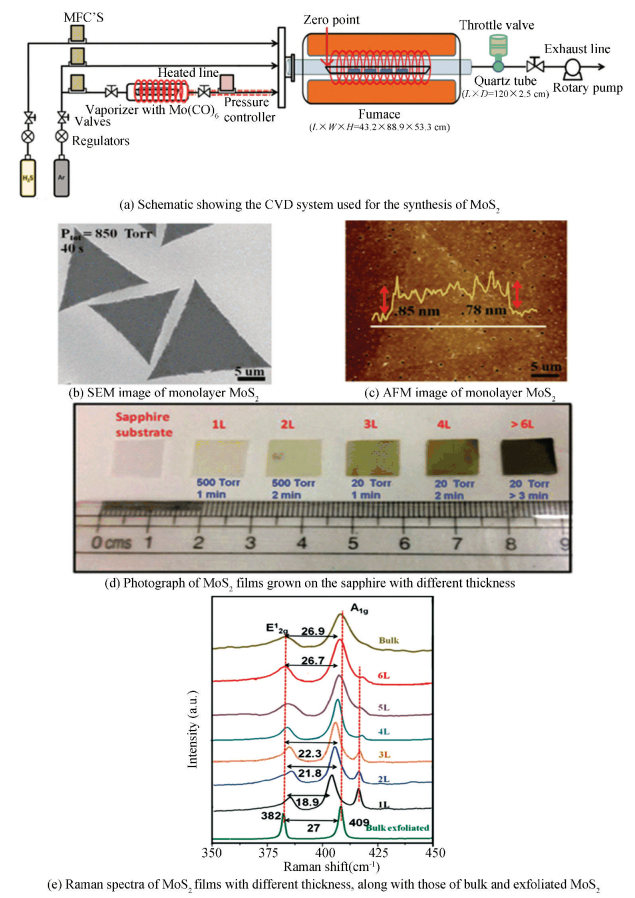 Figure 19 Controllable synthesis of layered MoS2 by using Mo(CO)6 and H2S as precursors[67]
 According to the above discussion, it is very clear to see that the species of Mo precursors are extremely vital to the growth of high quality MoS2 since various Mo precursors have different sublimation temperatures, that means, during the growth process, the vapor concentration of Mo species above the substrates is diverse, which will determine the nucleation density of MoS2. Generally, achieving a relatively low nucleation density is favorable to decrease the grain boundaries and improve the quality of the obtained MoS2. Moreover, compared to solid and liquid Mo precursors, selecting a gaseous precursor like Mo(CO)6 will make the synthesis process more controllable, for which is introduced into the reaction chamber in the form of vapor phase, thus we can easily control the concentration of the precursor and then reduce nucleation to form high quality MoS2 films. In addition, during the growth of layered MoS2, the Mo precursors should evaporate continuously to feed Mo source in the gas phase for achieving large size single-crystal MoS2 domains and to avoid being poisoned.
3 Conclusion and Perspectives At present, atomically thin MoS2 has been achieved by various "top-down" and "bottom up" strategies, and applied in many fields, such as electrical, optical, catalysis and photovoltaic devices. Notably, atomically thin MoS2 layer exhibits great potential of being fabricated into electronics due to its semi-conductive property, which is one of the primary advantages of MoS2 over graphene, since the zero bandgap makes graphene not suitable for the fabrication of logic circuits. Thus, MoS2-based electronics show great potential for future applications. In addition, stacking other kinds of 2D materials with MoS2 for the research of new properties or phenomena has also attracted a lot of interest. Thus, developing a simple, controllable and scalable method to synthesize high quality MoS2 is of great importance for future applications. As we all know, the CVD method is a preponderant bottom-up strategy used to prepare atomically thin nanomaterials in terms of scalability, simple operation and low cost, which are suitable for electronic and optoelectronic devices. Bearing this in mind, we provided a systematical overview about the preparation of single or few layered MoS2 by CVD in recent years and highlighted that we can achieve high-quality single or few layered MoS2 by engineering the main experiment parameters like growth substrates, carrier gases and Mo precursors for future various applications.
References
[1] Zhang H. Ultrathin two-dimensional nanomaterials. ACS Nano, 2015, 9(10): 9451-9469. DOI:10.1021/acsnano.5b05040 (
 0)
0)[2] Tan C, Cao X, Wu X J, et al. Recent advances in ultrathin two-dimensional nanomaterials. Chemical Reviews, 2017, 117(9): 6225-6331. DOI:10.1021/acs.chemrev.6b00558 (
 0)
0)[3] Novoselov K S, Mishchenko A, Carvalho A, et al. 2D materials and van der Waals heterostructures. Science, 2016, 353(6298): aac9439. DOI:10.1126/science.aac9439 (
 0)
0)[4] Hong J, Jin C, Yuan J, et al. Atomic defects in two-dimensional materials: From single-atom spectroscopy to functionalities in opto-/electronics, nanomagnetism, and catalysis. Advanced Materials, 2017, 29(14): 1606434. DOI:10.1002/adma.201606434 (
 0)
0)[5] Chhowalla M, Shin H S, Eda G, et al. The chemistry of two-dimensional layered transition metal dichalcogenide nanosheets. Nature Chemistry, 2013, 5(4): 263-275. DOI:10.1038/nchem.1589 (
 0)
0)[6] Tan C, Zhang H. Two-dimensional transition metal dichalcogenide nanosheet-based composites. Chemical Society Reviews, 2015, 44(9): 2713-2731. DOI:10.1039/c4cs00182f (
 0)
0)[7] Xu M, Liang T, Shi M, et al. Graphene-like two-dimensional materials. Chemical Reviews, 2013, 113(5): 3766-3798. DOI:10.1021/cr300263a (
 0)
0)[8] Li X G, Tao Y, Li F R, et al. Efficient preparation and characterization of functional graphene with versatile applicability. Journal of Harbin Institute of Technology (New Series), 2016, 23(3): 1-29. DOI:10.11916/j.issn.1005-9113.2016.03.001 (
 0)
0)[9] Zheng J, Yan X, Lu Z, et al. High-mobility multilayered MoS2 flakes with low contact resistance grown by chemical vapor deposition. Advanced Materials, 2017, 29(13): 1604540. DOI:10.1002/adma.201604540 (
 0)
0)[10] Desai S B, Madhvapathy S R, Sachid A B, et al. MoS2 transistors with 1-nanometer gate lengths. Science, 2016, 354(6308): 99-102. DOI:10.1126/science.aah4698 (
 0)
0)[11] Yan C, Gan L, Zhou X, et al. Space-confined chemical vapor deposition synthesis of ultrathin HfS2 flakes for optoelectronic application. Advanced Functional Materials, 2017, 27(39): 1702918. DOI:10.1002/adfm.201702918 (
 0)
0)[12] Tsai Y, Chu Z, Han Y, et al. Tailoring semiconductor lateral multijunctions for giant photoconductivity enhancement. Advanced Materials, 2017, 29(41): 1703680. DOI:10.1002/adma.201703680 (
 0)
0)[13] Shi J, Wang X, Zhang S, et al. Two-dimensional metallic tantalum disulfide as a hydrogen evolution catalyst. Nature Communications, 2017, 8(1): Article number:958. DOI:10.1038/s41467-017-01089-z (
 0)
0)[14] Ying Y, Zhang Y, Gao T, et al. Synergistic phase and disorder engineering in 1T-MoSe2 nanosheets for enhanced hydrogen-evolution reaction. Advanced Materials, 2017, 29(28): 1700311. DOI:10.1002/adma.201700311 (
 0)
0)[15] Liu Z, Lau S P, Yan F. Functionalized graphene and other two-dimensional materials for photovoltaic devices: Device design and processing. Chemical Society Reviews, 2015, 44(15): 5638-5679. DOI:10.1039/C4CS00455H (
 0)
0)[16] Singh E, Kim K S, Yeom G Y, et al. Two-dimensional transition metal dichalcogenide-based counter electrodes for dye-sensitized solar cells. RSC Advances, 2017, 7(45): 28234-28249. DOI:10.1039/c7ra03599c (
 0)
0)[17] Splendiani A, Sun L, Zhang Y, et al. Emerging photoluminescence in monolayer MoS2. Nano Letters, 2010, 10(4): 1271-1275. DOI:10.1021/nl903868w (
 0)
0)[18] Mak K F, Lee C, Hone J, et al. Atomically thin MoS2: A new direct-gap semiconductor. Phys. Rev. Lett., 2010, 105(13): 136805. DOI:10.1103/PhysRevLett.105.136805 (
 0)
0)[19] Radisavljevic B, Radenovic A, Brivio J, et al. Single-layer MoS2 transistors. Nature Nanotechnology, 2011, 6(3): 147-150. DOI:10.1038/nnano.2010.279 (
 0)
0)[20] Yin Z, Li H, Li H, et al. Single-layer MoS2 phototransistors. ACS Nano, 2012, 6(1): 74-80. DOI:10.1021/nn2024557 (
 0)
0)[21] Pezeshki A, Shokouh S H H, Jeon P J, et al. Static and dynamic performance of complementary inverters based on nanosheet α-MoTe2 p-channel and MoS2 n-channel transistors. ACS Nano, 2016, 10(1): 1118-1125. DOI:10.1021/acsnano.5b06419 (
 0)
0)[22] Lee C, Yan H, Brus L E, et al. Anomalous lattice vibrations of single- and few-layer MoS2. ACS Nano, 2010, 4(5): 2695-2700. DOI:10.1021/nn1003937 (
 0)
0)[23] Coleman J N, Lotya M, O'Neill A, et al. Two-dimensional nanosheets produced by liquid exfoliation of layered materials. Science, 2011, 331(6017): 568-571. DOI:10.1126/science.1194975 (
 0)
0)[24] Cunningham G, Lotya M, Cucinotta C S, et al. Solvent exfoliation of transition metal dichalcogenides: Dispersibility of exfoliated nanosheets varies only weakly between compounds. ACS Nano, 2012, 6(4): 3468-3480. DOI:10.1021/nn300503e (
 0)
0)[25] Ramakrishna Matte H S S, Gomathi A, Manna A K, et al. MoS2 and WS2 analogues of graphene. Angewandte Chemie International Edition, 2010, 49(24): 4059-4062. DOI:10.1002/anie.201000009 (
 0)
0)[26] Miremadi B K, Cowan T, Morrison S R. New structures from exfoliated MoS2. Journal of Applied Physics, 1991, 69(9): 6373-6379. DOI:10.1063/1.348839 (
 0)
0)[27] Hsieh K, Kochat V, Xiang Z, et al. Effect of carrier localization on electrical transport and noise at individual grain boundaries in monolayer MoS2. Nano Letters, 2017, 17(9): 5452-5457. DOI:10.1021/acs.nanolett.7b02099 (
 0)
0)[28] Zhan Y, Liu Z, Najmaei S, et al. Large-area vapor-phase growth and characterization of MoS2 atomic layers on a SiO2 substrate. Small, 2012, 8(7): 966-971. DOI:10.1002/smll.201102654 (
 0)
0)[29] Najmaei S, Liu Z, Zhou W, et al. Vapour phase growth and grain boundary structure of molybdenum disulphide atomic layers. Nature Materials, 2013, 12: 754-759. DOI:10.1038/NMAT3673 (
 0)
0)[30] Zhao X, Fu D, Ding Z, et al. Mo-terminated edge reconstructions in nanoporous molybdenum disulfide film. Nano Letters, 2017, 18(1): 482-490. DOI:10.1021/acs.nanolett.7b04426 (
 0)
0)[31] Fu D, Zhao X, Zhang Y Y, et al. Molecular beam epitaxy of highly crystalline monolayer molybdenum disulfide on hexagonal boron nitride. Journal of the American Chemical Society, 2017, 139(27): 9392-9400. DOI:10.1021/jacs.7b05131 (
 0)
0)[32] Yan Y, Xia B Y, Li N, et al. Vertically oriented MoS2 and WS2 nanosheets directly grown on carbon cloth as efficient and stable 3-dimensional hydrogen-evolving cathodes. Journal of Materials Chemistry A, 2014, 3(1): 131-135. DOI:10.1039/C4TA04858J (
 0)
0)[33] Wang Y, Yu L, Lou X W. Synthesis of highly uniform molybdenum-glycerate spheres and their conversion into hierarchical MoS2 hollow nanospheres for lithium-ion batteries. Angewandte Chemie International Edition, 2016, 55(26): 7423-7426. DOI:10.1002/anie.201601673 (
 0)
0)[34] Xie J, Zhang H, Li S, et al. Defect-rich MoS2 ultrathin nanosheets with additional active edge sites for enhanced electrocatalytic hydrogen evolution. Adv. Mater., 2013, 25(40): 5807-5813. DOI:10.1002/adma.201302685 (
 0)
0)[35] Xie J F, Zhang J J, Li S, et al. Controllable disorder engineering in oxygen-incorporated MoS2 ultrathin nanosheets for efficient hydrogen evolution. Journal of American Chemical Society, 2013, 135(47): 17881-17888. DOI:10.1021/ja408329q (
 0)
0)[36] Hu D, Xu G, Xing L, et al. Two-dimensional semiconductors grown by chemical vapor transport. Angewandte Chemie International Edition, 2017, 56(13): 3611-3615. DOI:10.1002/anie.201700439 (
 0)
0)[37] Kalanyan B, Kimes W A, Beams R, et al. Rapid wafer-scale growth of polycrystalline 2H-MoS2 by pulsed metal-organic chemical vapor deposition. Chemistry of Materials, 2017, 29(15): 6279-6288. DOI:10.1021/acs.chemmater.7b01367 (
 0)
0)[38] Kim T, Mun J, Park H, et al. Wafer-scale production of highly uniform two-dimensional MoS2 by metal organic chemical vapor deposition. Nanotechnology, 2017, 28(18): 18LT01. DOI:10.1088/1361-6528/aa6958 (
 0)
0)[39] Novoselov K S, Geim A K, Morozov S V, et al. Electric field effect in atomically thin carbon films. Science, 2004, 306(5696): 666-669. DOI:10.1126/science.1102896 (
 0)
0)[40] Lin Z, Mccreary A, Briggs N, et al. 2D materials advances: from large scale synthesis and controlled heterostructures to improved characterization techniques, defects and applications. 2D Materials, 2016, 3(4): 042001. DOI:10.1088/2053-1583/3/4/042001 (
 0)
0)[41] Shi J P, Zhou X B, Zhang Z P, et al. Controllable syntheses and energy related applications of MX2 heterostructures. Chinese Science Bulletin, 2017, 62(20): 2180-2194. DOI:10.1360/N972016-01387 (
 0)
0)[42] Ji Q, Zhang Y, Gao T, et al. Epitaxial monolayer MoS2 on mica with novel photoluminescence. Nano Letters, 2013, 13(8): 3870-3877. DOI:10.1021/nl401938t (
 0)
0)[43] Ji Q, Kan M, Zhang Y, et al. Unravelling orientation distribution and merging behavior of monolayer MoS2 domains on sapphire. Nano Letters, 2015, 15(1): 198-205. DOI:10.1021/nl503373x (
 0)
0)[44] Dumcenco D, Ovchinnikov D, Marinov K, et al. Large-Area Epitaxial Monolayer MoS2. ACS Nano, 2015, 9(4): 4611-4620. DOI:10.1021/acsnano.5b01281 (
 0)
0)[45] Zhang Y, Ji Q, Han G F, et al. Dendritic, transferable, strictly monolayer MoS2 flakes synthesized on SrTiO3 single crystals for efficient electrocatalytic applications. ACS Nano, 2014, 8(8): 8617-8624. DOI:10.1021/nn503412w (
 0)
0)[46] Li C, Zhang Y, Ji Q, et al. Substrate effect on the growth of monolayer dendritic MoS2 on LaAlO3 (100) and its electrocatalytic applications. 2D Materials, 2016, 3(3): 035001. DOI:10.1088/2053-1583/3/3/035001 (
 0)
0)[47] Shi J, Ma D, Han G F, et al. Controllable growth and transfer of monolayer MoS2 on Au foils and its potential application in hydrogen evolution reaction. ACS Nano, 2014, 8(10): 10196-10204. DOI:10.1021/nn503211t (
 0)
0)[48] Shi J, Zhang X, Ma D, et al. Substrate Facet Effect on the growth of monolayer MoS2 on Au foils. ACS Nano, 2015, 9(4): 4017-4025. DOI:10.1021/acsnano.5b00081 (
 0)
0)[49] Li X G, Huang M R, Bai H, et al. Thermogravimetry of thermoplastic polyimide powders under four different atmospheres. Macromolecular Materials and Engineering, 2001, 286(7): 421-428. DOI:10.1002/(ISSN)1439-2054 (
 0)
0)[50] Gong Y, Li B, Ye G, et al. Direct growth of MoS2 single crystals on polyimide substrates. 2D Materials, 2017, 4: 021028. DOI:10.1088/2053-1583/aa6fd2 (
 0)
0)[51] Lee Y H, Zhang X Q, Zhang W, et al. Synthesis of large-area MoS2 atomic layers with chemical vapor deposition. Advanced Materials, 2012, 24(17): 2320-2325. DOI:10.1002/adma.201104798 (
 0)
0)[52] Lee Y H, Yu L, Wang H, et al. Synthesis and transfer of single-layer transition metal disulfides on diverse surfaces. Nano Letters, 2013, 13(4): 1852-1857. DOI:10.1021/nl400687n (
 0)
0)[53] Ling X, Lee Y H, Lin Y, et al. Role of the seeding promoter in MoS2 growth by chemical vapor deposition. Nano Letters, 2014, 14(2): 464-472. DOI:10.1021/nl4033704 (
 0)
0)[54] Jeon J, Jang S K, Jeon S M, et al. Layer-controlled CVD growth of large-area two-dimensional MoS2 films. Nanoscale, 2015, 7(5): 1688-1695. DOI:10.1039/C4NR04532G (
 0)
0)[55] Song I, Park C, Hong M, et al. Patternable large-scale molybdenium disulfide atomic layers grown by gold-assisted chemical vapor deposition. Angewandte Chemie International Edition, 2014, 53(5): 1266-1269. DOI:10.1002/anie.201309474 (
 0)
0)[56] Chen W, Zhao J, Zhang J, et al. Oxygen-assisted chemical vapor deposition growth of large single-crystal and high-quality monolayer MoS2. Journal of the American Chemical Society, 2015, 137(50): 15632-15635. DOI:10.1021/jacs.5b10519 (
 0)
0)[57] Yu H, Liao M, Zhao W, et al. Wafer-scale growth and transfer of highly-oriented monolayer MoS2 continuous films. ACS Nano, 2017, 11(12): 12001-12007. DOI:10.1021/acsnano.7b03819 (
 0)
0)[58] Shi J, Yang Y, Zhang Y, et al. Monolayer MoS2 growth on Au foils and on-site domain boundary imaging. Advanced Functional Materials, 2015, 25(6): 842-849. DOI:10.1002/adfm.201403659 (
 0)
0)[59] Tai G, Zeng T, Yu J, et al. Fast and large-area growth of uniform MoS2 monolayers on molybdenum foils. Nanoscale, 2016, 8(4): 2234-2241. DOI:10.1039/C5NR07226C (
 0)
0)[60] Robertson J, Liu X, Yue C, et al. Wafer-scale synthesis of monolayer and few-layer MoS2 via thermal vapor sulfurization. 2D Materials, 2017, 4(4): 045007. DOI:10.1088/2053-1583/aa8678 (
 0)
0)[61] Li D, Xiao Z, Mu S, et al. A facile space-confined solid-phase sulfurization strategy for growth of high-quality ultrathin molybdenum disulfide single crystals. Nano Lett, 2018(3): 2021-2032. DOI:10.1021/acs.nanolett.7b05473 (
 0)
0)[62] Lin Y C, Zhang W, Huang J K, et al. Wafer-scale MoS2 thin layers prepared by MoO3 sulfurization. Nanoscale, 2012, 4(20): 6637-6641. DOI:10.1039/C2NR31833D (
 0)
0)[63] Lee J, Pak S, Giraud P, et al. Thermodynamically stable synthesis of large-scale and highly crystalline transition metal dichalcogenide monolayers and their unipolar n-n heterojunction devices. Advanced Materials, 2017, 29(33): 1702206. DOI:10.1002/adma.201702206 (
 0)
0)[64] Wang X, Feng H, Wu Y, et al. Controlled synthesis of highly crystalline MoS2 flakes by chemical vapor deposition. Journal of the American Chemical Society, 2013, 135(14): 5304-5307. DOI:10.1021/ja4013485 (
 0)
0)[65] Yu Y, Li C, Liu Y, et al. Controlled scalable synthesis of uniform, high-quality monolayer and few-layer MoS2 films. Scientific Report, 2013, 3(5): 1866. DOI:10.1038/srep01866 (
 0)
0)[66] Liu K K, Zhang W, Lee Y H, et al. Growth of large-area and highly crystalline MoS2 thin layers on insulating substrates. Nano Letters, 2012, 12(3): 1538-1544. DOI:10.1021/nl2043612 (
 0)
0)[67] Kranthi Kumar V, Dhar S, Choudhury T H, et al. A predictive approach to CVD of crystalline layers of TMDs: The case of MoS2. Nanoscale, 2015, 7(17): 7802-7810. DOI:10.1039/C4NR07080A (
 0)
0)