 ,3, Mehran Shahmansouri,1Department of Physics, Faculty of Science,
 2Institute of Advanced Technology,
First author contact:
Received:2019-08-26Revised:2020-01-14Accepted:2020-02-03Online:2020-03-16

Abstract
KeywordsЃК
PDF (423KB)MetadataMetricsRelated articlesExportEndNote|Ris|BibtexFavorite
Cite this article
Raheleh Aboltaman, Mehran Shahmansouri. Boundary graphene layer effect on surface plasmon oscillations in a quantum plasma half-space. Communications in Theoretical Physics, 2020, 72(4): 045501- doi:10.1088/1572-9494/ab76fc
1. Introduction
The physical characteristics of surface waves has attracted a great interest in theoretical, numerical, and experimental investigations in many fields of plasma science and technology such as plasma spectroscopy, surface science, nano- electronic devices with surface Plasmons which can be excited and transmitted in metal thin films, laser physics, overdense plasma heating and so on [1–10]. These waves can propagate along the boundary of two different mediums with different signs of the real part of dielectric response function [11] and evanescent on either side of it. The existence of the linear electrostatic surface oscillations was first proved for a cold plasma half-space by Ritchie in 1957 [12] and for a cold cylindrical plasma columns by Trivelpiece and Gould in 1959 [13]. The effects of finite plasma temperature have also been considered [14–17] and the propagation of the surface waves on an unmagnetized quantum plasma half-space has been investigated by employing the quantum hydrodynamic (QHD) model which obtained from self-consistent Hartree equations [18] or from the phase-space Wigner–Poisson equations [19] conjugating with Maxwell–Poisson equations by Lazar et al [16] and Shahmansouri [17].The electrostatic surface oscillations of free electrons near a plasma-dielectric surface is called surface Plasmon (SP) and it’s linear coupling with photons is considered as a hybrid surface mode called surface Plasmon Polariton (SPP). SPs can provide a way of confining electromagnetic field to nanoscale structures and SPPs can be excited at frequencies ranging from 0 up to ${\omega }_{{\rm{p}}{\rm{e}}}/\sqrt{2}$ (in which ${\omega }_{{\rm{p}}{\rm{e}}}$ considered as the plasma frequency).
The quantum Fermi temperature and quantum electron tunneling (Bohm potential) effects should be considered, due to the great degree of miniaturization of nowadays electronic devices and also high number density in metallic plasmas or in solid-density plasma. On the other hand, the quantum effects can no longer be neglected since the thermal deBroglie wavelength of electrons is comparable to the average interparticle distance of them. The dispersion relation of surface waves is profoundly affected by both the quantum Fermi temperature and quantum electron tunneling effects [16, 17]. This is the case that makes the behavior of surface waves on quantum plasma half-space as an important issue in recent years. The fundamental properties of the surface waves in quantum plasma have been studied in the previous investigations [10, 16–33] under the influence of e.g. the quantum tunneling [10, 20–31], external magnetic field [20–22], collisional effects [24, 25], relativistic effects [26], spins [27–30], nonlocality effects [31] and exchange effects [17, 32 and 33].
A surprising property of graphene [34–43], a two dimensional (2D) monolayer of carbon atoms tightly packed in a hexagonal lattice, has attracted a great deal of attention for a wide range of electronic and electromagnetic applications. Interaction of the electrons with this wonderful atomic structure forces the charge carriers in graphene to act as an effective zeromass particle which can show photon-like dispersion in the low energy excitations [44]. The unique electron structure in which conduction and valance bands meet each other at the Dirac point is the origin of the extraordinary optical properties of graphene. The property of graphene can be tuned by chemical doping or electrical gating due to change in the value of the chemical potential ${\mu }_{{\rm{c}}}$ or Fermi level ${E}_{{\rm{f}}}$ of graphene. The complex dynamic optical response of graphene consisting of interband and intraband contributions can be derived from Kubo formula [45–48]. By changing in the level of chemical potential, the imaginary part of conductivity can achieve negative and positive values [48], in different ranges of frequencies.
Here, only the intraband conductivity which dominates the low frequency process of graphene transition is included. Therefore, the optical conductivity of graphene (${\sigma }_{{\rm{g}}}\approx {\sigma }_{{\rm{i}}{\rm{n}}{\rm{t}}{\rm{r}}{\rm{a}}}$) is defined as follow [49–53]:
In which $\omega $ is frequency of the incident light, T is temperature, ${k}_{{\rm{B}}}$ is Boltzmann constant, $\tau $ is relaxation time and, ${\mu }_{{\rm{c}}}$ is chemical potential. For the gated or highly doped graphene ($\left|{\mu }_{{\rm{c}}}\right|\gg {k}_{{\rm{B}}}T$), the interband terms of the graphene conductivity have form [46]:
Recent investigations reveal that low-cost metal-graphene composites [54–57] are promising materials in high-power electronics applications and can be widely used in digital and nanoelectronic devices. The bonding of graphene to metal substrates can be classified into two groups [54, 56]: (i) physisorption, in which the interaction between graphene and metals, such as Ag, Au, Cu, Al and Pt(111) is weak and preserves the graphene’s linear dispersion band and Dirac cone. This weak adsorption on metal surfaces causes the Fermi level to shift from the conical points in graphene, leading to doping with either electrons or holes [56]. The difference of the graphene and metal work functions is the origin of this doping. The downward (upward) shift of Fermi-level means that holes (electrons) are transfer from the metal substrate to graphene (in order to equilibrate the Fermi levels), which causes p-type (n-type) doping. Graphene is p-type on Au and Pt and n-type on Ag, Al and Cu. (ii) chemisorptions, the metals Co, Ni and Pd bind graphene so strong that the electronic characteristics of graphene (the characteristic conical point at K) are disturbed. In this work we study the Au-graphene structure in which the basic characteristics of graphane remain unchanged. The rapid progress in this field necessitates a fundamental study of their interfacial structural and electronic coupling, which could be the key issue to determine their performance for engineering applications [54], for more information see [54–58].
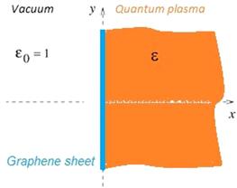
In this work, we investigate the effect of a graphene sheet which exactly placed on the boundary of quantum plasma half-space and vacuum (see figure 1), on the dispersion relation of the plasma surface waves (SPPs).
Figure 1.
 New window|Download| PPT slide
Figure 1.Schematic diagram of a quantum plasma half-space: the graphene sheet is located on the interface of plasma-vacuum at the plane x = 0, and the surface wave is propagating along the interface on y axis.
The outline of this paper is as follows: after introduction, in section
2. Theoretical model
In grphene, two kinds of electrons named $\sigma $ and $\pi $ electrons can support Plasmons. 2D Plasmons (also named low energy Plasmons with energy <3 eV) which is responsible for intraband transitions, can appear in doped graphene while two other kinds of Plasmons (named as $\pi $ and $\pi +\sigma $) exist in pristine graphene and also in higher energies ($\gt 3\,{\rm{eV}}$) [58]. An interested frequency range for our model, cannot excite these two types of Plasmons in graphene, therefore we just focus on the metal (quantum plasma half-space) Plasmons. To investigate the dispersion properties in a quasineutral collisionless quantum plasma half-space (shown in figure 1) consisting of motionless ions (as a neutralizing background) and fluid electrons, we use a macroscopic approach based on the linearized fluid equations, which is valid just in the weak ${r}_{{\rm{s}}}\leqslant 0.1$ and moderate $0.1\lt {r}_{{\rm{s}}}\leqslant 1$ coupling (in which ${r}_{{\rm{s}}}={e}^{2}/\hslash {v}_{{\rm{F}}}$ is a quantum coupling parameter or fine structure constant) [43], including the quantum statistical pressure and the quantum electron tunneling (the second and the third term in equation (In which n ($\ll {n}_{0}$) is a small electron density perturbation in the equilibrium number density ${n}_{0},$ e is the magnitude of the electron charge, m is the electron mass and the perturbed quantities v, E and B are respectively the electron fluid velocity, the electric and magnetic fields. The surface wave propagates on the interface (which covered by a graphene layer) along the y axis. We will study the surface transverse magnetic (TM) wave so the field components are given by ${\boldsymbol{E}}=\left({E}_{x},{E}_{y},0\right)$ and ${\boldsymbol{B}}=\left(0,0,{B}_{z}\right).$ In the following, by assuming that all the physical quantities vary as $\psi \left(x\right)\exp ({\rm{i}}{k}_{y}y-{\rm{i}}\omega t)$ in which $\psi \left(x\right)\,\equiv $ [$N\left(x\right);{U}_{x}\left(x\right);{U}_{y}\left(x\right);$ ${E}_{x}\left(x\right);{E}_{y}\left(x\right);{B}_{z}\left(x\right)$] and by employing the time-space Fourier transformation of equations (
Then, the second-order differential equation for the magnetic field can be obtained by employing the Maxwell equations (
Equations (
In the aforementioned equations, ${{\boldsymbol{D}}}_{1}$ and ${{\boldsymbol{D}}}_{2}$ are constants given by ${{\boldsymbol{D}}}_{1}={B}_{1}(-c\omega /{k}_{y}{\omega }^{2})({k}_{y}^{2}\hat{i}+{\rm{i}}{q}_{v}{k}_{y}\hat{j})$ and ${{\boldsymbol{D}}}_{2}={B}_{2}(c\omega /{k}_{y}({\omega }_{{\rm{p}}{\rm{e}}}^{2}-{\omega }^{2}))({k}_{y}^{2}\hat{{i}}-{\rm{i}}{q}_{p}{k}_{y}\hat{j}),$ respectively.
In what follows, we just keep that part of solutions which disappear by moving away from the boundary in both regions. The boundary conditions for the electromagnetic field components will be modified by the existence of graphene sheet with conductivity ${\sigma }_{{\rm{g}}}$ on the plasma-vacuum interface, in the following form:
By using the above matching conditions together with the boundary condition ${v}_{x}=0$ at x=0 for the electron velocity, the dispersion relation of the surface modes on our quantum plasma half-space system can be derived as follow:
To our knowledge, this is the first time that a dispersion relation of SPP mode on a quantum plasma half-space with a graphene sheet on the interface has been derived. In the absence of graphene (${\sigma }_{{\rm{g}}}\to 0$) this dispersion relation leads to that obtained by Kaw and McBride [15] (in the absence of quantum corrections) and Lazar et al [16] results. In the following we assume overcritical density plasmas (which happen in solid state plasma such as metals and semiconductors) by letting (${k}_{y}^{2}{v}_{{\rm{F}}{\rm{e}}}^{2}+{\hslash }^{2}{k}_{y}^{4}/4{m}^{2}\ll \left|{\omega }_{{\rm{p}}{\rm{e}}}^{2}-{\omega }^{2}\right|$), and then equation (
Since in the standard metallic densities [59], quantum effects do not affect the transverse electromagnetic component of the surface modes, we restrict our attention to the electrostatic part of the surface waves only. In the electrostatic limit, or when $c\to \infty ,$ the general dispersion relation (
Without quantum effects and in the absence of graphene sheet, equation (
3. Numerical analysis
By introducing the dimensionless quantities: $W=\omega /{\omega }_{{\rm{p}}{\rm{e}}},$ $\Im =({\omega }_{{\rm{p}}{\rm{e}}}\tau ),$ $K={k}_{y}{v}_{{\rm{F}}{\rm{e}}}/{\omega }_{{\rm{p}}{\rm{e}}}$ and the Plasmonic coupling parameter as $H=\hslash {\omega }_{{\rm{p}}{\rm{e}}}/2{m}_{{e}}{v}_{{\rm{F}}{\rm{e}}}^{2},$ equation (In which the normalized conductivity ${\bar{\sigma }}_{{\rm{g}}}$ define as ${\bar{\sigma }}_{{\rm{g}}}={\rm{i}}\beta \xi /\left(W+2{\rm{i}}{\Im }^{-1}\right)$ where $\xi ={e}^{2}{k}_{{\rm{B}}}T/{\hslash }^{2}{v}_{{\rm{F}}}{\omega }_{{\rm{p}}{\rm{e}}}$ and $\beta \,=({\mu }_{{\rm{c}}}/{k}_{{\rm{B}}}T)+2\,\mathrm{ln}\left(\exp (-{\mu }_{{\rm{c}}}/{k}_{{\rm{B}}}T)+1\right).$
We depict equation (
The above expression shows that the normalized conductivity becomes a pure imaginary (pure real) quantity for $W\Im \gg 1$ ($W\Im \ll 1$). In this case the wave frequency reduced to the following form as
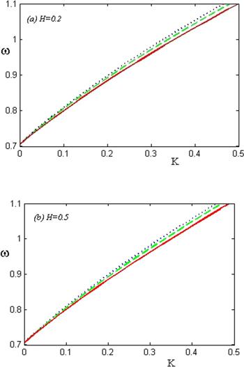
Then, in order to see how the frequency wave may be affected by the presence of the thin graphene layer, the normalized wave frequency W is depicted in figures 2 and 3, for different values of $\beta \xi $ and $H,$ respectively.
Figure 2.
 New window|Download| PPT slide
Figure 2.The normalized frequency of the surface plasmon waves W with respect to the normalized wave number K, for (a) H=0.2 and (b) H=0.5, and different values of parameter $\beta \xi ,$ as solid line refers to $\beta \xi =0,$ dashed line refers to $\beta \xi =0.11,$ and dotted line refer to $\beta \xi =0.2.$
Figure 3.
 New window|Download| PPT slide
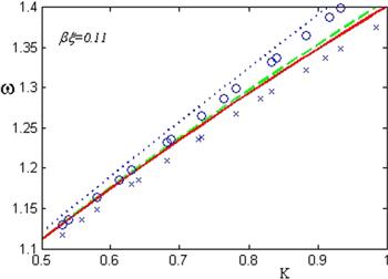
Figure 3.The normalized frequency of the surface Plasmon waves W with respect to the normalized wave number K, for different values of the Plasmonic coupling parameter H, as solid line refers to $H=0.1,$ dashed line refers to $H=0.2,$ and dotted line refer to $H=0.5.$ In this case $\beta \xi =0.11.$
Figure 2 represents the normalized wave frequency $W$ of surface waves as a function of the normalized wavenumber $K,$ in the presence of graphene layer for different values of the parameter $\beta \xi .$ This figure represents that the frequency of surface Plasmon waves experiences an enhancement due to the presence of boundary graphene layer. For better comparison the Lazar et al [16] limit is included in this figure (solid line). The up-shift of the wave frequency increases with magnitude of the conductivity coefficient. The effect of the Plasmonic coupling parameter is included in panels (a) and (b) of figure 2. It is obvious that the wave frequency for higher values of $H$ is takes greater values.
To see an obvious influence of the quantum effects on the wave frequency, figure 3 is depicted for different values of $H,$ beside the limits of Lazar et al [16] (marker o) and Ritchie [14] (marker ×), for $\beta \xi =0.11.$ It can be seen that the quantum effects beside the presence of boundary graphene layer cause to increase the wave frequency. Therefore, inclusion of the boundary graphene layer and quantum effects makes the Plasmon waves faster than that reported in the Ritchie limit [14].
It must be added that the results are significantly sensitive to the work frequency, as the graphene conductivity at high frequencies may be dominated by interband conductivity formulation. In this limit the effect of boundary graphene layer may be changed due to the interband conductivity.
4. Conclusions
In summary, we have employed a simple quantum hydrodynamic approach to investigate the dispersion properties of surface Plasmon waves in semi-infinite plasma in the presence of a boundary graphene layer. In this context, all the previous results are also recovered. At first approximation the garaphene layer leads to discreteness in electromagnetic fields at interface of plasma-vacuum. For typical numerical parameters corresponding to gold metal [16], the presence of graphene layer enhances the wave frequency as well as the phase velocity. This up-shift is similar to that causes by the quantum effects. Thus, inclusion of boundary graphene layer and quantum effects significantly affect the wave frequency relative to the Ritchie limit. Consideration of different physical parameters that yield other interesting plasma situations (such as degenerate plasma, relativistic plasma, etc) can be a problem of interest, but is beyond of the scope of the present study. Also, the coupling between the Plasmons in graphene and plasma regions may be left for future investigation. The results of present study must be contributed to the surface plasma and modern nano-electronic investigations.Reference By original order
By published year
By cited within times
By Impact factor
DOI:10.1002/ctpp.19860260210 [Cited within: 1]
DOI:10.1088/0031-8949/1996/T63/008
DOI:10.1007/978-3-642-57060-5
DOI:10.1063/1.1555625
DOI:10.1007/s00339-016-0574-x
DOI:10.1088/0253-6102/71/4/435
DOI:10.1126/science.1071895
DOI:10.1016/B978-0-444-52838-4.X5000-0
DOI:10.1063/1.3649951
DOI:10.1017/S0022377809990055 [Cited within: 3]
DOI:10.1063/1.4793456 [Cited within: 1]
DOI:10.1103/PhysRev.106.874 [Cited within: 1]
DOI:10.1063/1.1735056 [Cited within: 1]
DOI:10.1143/PTP.29.607 [Cited within: 4]
DOI:10.1063/1.1693155 [Cited within: 1]
DOI:10.1063/1.2825278 [Cited within: 8]
DOI:10.1063/1.4930116 [Cited within: 4]
DOI:10.1090/fic/046/10 [Cited within: 1]
DOI:10.1103/PhysRevB.42.1240 [Cited within: 1]
DOI:10.1088/0031-8949/82/06/065502 [Cited within: 2]
DOI:10.1088/0031-8949/90/8/085601
DOI:10.1063/1.4960965 [Cited within: 1]
DOI:10.1103/PhysRevE.83.057401
DOI:10.1063/1.4843995 [Cited within: 1]
DOI:10.1063/1.3692771 [Cited within: 1]
DOI:10.1016/j.physleta.2013.05.003 [Cited within: 1]
DOI:10.1017/S0022377813000135 [Cited within: 1]
DOI:10.1017/S002237781400052X
DOI:10.1063/1.2737765
DOI:10.1063/1.4982740 [Cited within: 1]
DOI:10.1063/1.4906054 [Cited within: 2]
DOI:10.1063/1.4986333 [Cited within: 1]
DOI:10.1063/1.4955319 [Cited within: 2]
DOI:10.1038/nphoton.2010.186 [Cited within: 1]
DOI:10.1103/RevModPhys.83.851
DOI:10.1126/science.1102896
DOI:10.1007/s00339-017-1247-0
DOI:10.1038/nnano.2013.197
DOI:10.1038/nphys989
DOI:10.1103/RevModPhys.81.109
DOI:10.1063/1.4879017
DOI:10.1016/S1369-7021(13)70014-2
DOI:10.1016/j.physleta.2018.05.034 [Cited within: 2]
DOI:10.1007/s00339-017-1380-9 [Cited within: 1]
DOI:10.1103/PhysRevB.78.085432 [Cited within: 1]
DOI:10.1103/PhysRevB.75.165407 [Cited within: 1]
DOI:10.1021/nn300989g
DOI:10.1126/science.1202691 [Cited within: 2]
DOI:10.1103/PhysRevB.83.165113 [Cited within: 2]
DOI:10.1063/1.3698133
DOI:10.1063/1.2891452 [Cited within: 1]
DOI:10.1063/1.4879017
DOI:10.1038/nmat1849 [Cited within: 1]
DOI:10.1088/0953-8984/22/48/485301 [Cited within: 5]
DOI:10.1007/s00339-018-2236-7
[Cited within: 3]
DOI:10.1038/nmat2166 [Cited within: 1]
DOI:10.1140/epjb/e2015-60001-2 [Cited within: 2]
DOI:10.1103/PhysRevB.64.075316 [Cited within: 2]
