 ,1,4, Daxue Du2, Chunsheng Wang3, Zhaopeng Xu,1,41School of Information Science and Engineering, the Key Laboratory for Special Fiber and Fiber Sensor of Hebei Province,
 2School of Environment and Chemical Engineering,
3College of Vehicles and Energy,
First author contact:
Received:2019-08-10Revised:2019-10-17Accepted:2019-10-31Online:2020-01-10

Abstract
Keywords:
PDF (726KB)MetadataMetricsRelated articlesExportEndNote|Ris|BibtexFavorite
Cite this article
Chenbo Wang, Shuai Zhao, Fei Bian, Daxue Du, Chunsheng Wang, Zhaopeng Xu. Absorption enhancement of ultrathin crystalline silicon solar cells with frequency upconversion nanosphere arrays. Communications in Theoretical Physics, 2020, 72(1): 015501- doi:10.1088/1572-9494/ab5451
1. Introduction
To meet the huge energy problem and reduce carbon pollution that causes climate change, photovoltaic (PV) technology, as a clean and renewable power source, has now been widely studied. In many PV cells, crystalline silicon (c-Si) solar cells (SCs) still play an important role for their better performance in harvesting energy directly from sunlight [1]. However, the incomplete absorption of the incoming light poses a challenge to the widespread use of c-Si SCs [2]. One of the key factors to improve the efficiency in c-Si SCs is to enhance broadband antireflection (AR) [3]. Resonant dielectric structures are a promising platform for addressing the key challenge of broadband AR in c-Si SCs [4]. NSs arrays are attractive, owing to their low cost, high stability, tiny light loss and easy chemical modification [5]. When resonant NS AR coatings are placed on a silicon substrate, the resonant modes in the NSs show a significant increase in the optical path and in the absorption from leaking into the absorber layer [6]. Other researchers reported the AR effect of NSs coatings simulated by finite different time domain (FDTD) [7] and show that the difference in size of NSs results in different light trapping behaviors.Besides, about 20% of solar energy that reaches the Earth’s surface cannot be utilized by the silicon SCs because photons below the band-gap of silicon cannot transport enough energy to generate free charge carriers. Thus the upconversion (UC) of these low energy photons is a promising way to enhance the efficiency of SCs [8]. Detailed balance analyses indicate that the theoretical efficiency limit of silicon SCs can be pushed from near 30% to 40.2% via UC for the illumination of one sun [9]. For a long time, the host material sodium yttrium fluoride (NaYF4) has been known to provide high efficiency of UC [10]. For experimental realizations of silicon SCs with UC, cubic phase NaYF4 doped with 20% Er3+ (α-NaEr0.2Y0.8F4) has shown a comparatively high UC quantum yield in reasonably excitation intensities [11]. It can be learnt from the investigations that current research of SC light management technology mainly focuses on the light trapping of nanostructure arrays [12, 13] and the spectral conversion of frequency conversion materials [14, 15]. However, little attention was paid to combine the nanostructure with frequency UC for enhancing light trapping behaviors of SCs.
In this work, we proposed a structure of crystalline silicon SCs patterned with α-NaEr0.2Y0.8F4 NSs arrays on the surface as the antireflection layer and frequency UC layer. The light trapping performance of α-NaEr0.2Y0.8F4 NSs were systematically studied by COMSOL Multiphysics and the results show that the sphere nanostructures have better performance in reducing optical reflection and improving optical absorption. The combination of the nanostructure arrays with frequency UC materials can improve the light management and photoelectric conversion efficiency of c-Si SCs.
2. Methods and design
COMSOL Multiphysics was based on the finite element method and periodic boundary condition was applied in x- and y-directions while the perfect match layer was performed in the z-direction and absorbing boundary conditions were used at the top and bottom surface. Only a one-unit cell was required for the computational domain with proper periodic boundary conditions. The reflectance R(λ) and transmittance T(λ) were computed at each wavelength, thus the optical absorption A(λ) could be derived from A(λ)=1-R(λ)-T(λ). Perpendicular incident light of transverse electric (TE) and transverse magnetic (TM) waves were calculated separately and the average absorption was derived from the mean value of the absorption of TE and TM modes.Simulations were carried out at the wavelength range of 300–1150 nm with a 10 nm step size and the short circuit current density (Jsc) is calculated from the equation as follows:
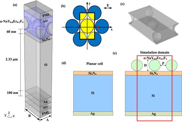
As depicted in figure 1, a single unit cell with a layer of flat Si3N4 anti-reflection coating on the surface was designed for where λg is the corresponding wavelength of the Si bandgap, i.e., 1127 nm, I(λ) is the standard solar irradiance spectrum of AM 1.5G, A(λ) is the optical absorption of the structure at the wavelength λ, e is the elementary charge, h is the Planck’s constant, c is the velocity of light in vacuum [16]. Comparative analysis: the active layer was made of 2.33 μm thickness c-Si referring to [17, 18]. On the bottom, a 100 nm thick silver layer was placed as a back reflector that reflects back most of the unabsorbed incident sunlight [19]. The α-NaEr0.2Y0.8F4 NSs were packed on the surface of c-Si as a dielectric layer and up-conversion materials. Refractive indices of Si3N4, c-Si and Ag were taken from previously measured data, respectively [20, 21], while the complex refractive indices of α-NaEr0.2Y0.8F4 were calculated by a plane-wave pseudo potential DFT-based software CASTEP code [22]. To reduce simulation time, a small unit of hexagonally packed NSs was modeled. The minimum basic unit was rectangular A×B, which was illustrated in figure 1(a). The lattice constant A was equal to the diameter of the NSs, while B was 1.732 times than that of A [23]. There was spacing between NSs and the pitch (P) represented the spacing between the NSs. We defined f as the ratios of D to P for the following calculation.
Figure 1.
 New window|Download| PPT slide
Figure 1.(a) 3D diagram of the silicon SCs with 60 nm Si3N4 and hexagonally packed α-NaEr0.2Y0.8F4 NSs on the surface; (b) and (c) top view and oblique view of the periodic arrays of α-NaEr0.2Y0.8F4 NSs. The black rectangle of dimension indicates the lattice constant; (d) schematic of planar SCs with Si3N4 layer on the surface and Ag layer on the bottom; and (e) schematic of planar SCs with α-NaEr0.2Y0.8F4 NSs arrays on the surface.
3. Results and discussion
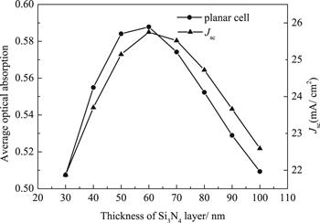
In order to find the best thickness of Si3N4 anti-reflection coating, we first investigated the influence of the Si3N4 layer on the bare silicon, which was only equipped with 100 nm Ag layer on the bottom. As figure 2 indicates, the 60 nm flat Si3N4 layer contributes to the largest average optical absorption and Jsc of c-Si SCs, reaching to 58.78% and 25.75 mA cm−2, respectively, which indicates that the 60 nm Si3N4 has the best matching light absorption coupling effect. The silicon SCs get the largest constructive interference in this thickness of theSi3N4 layer. In this case, the Si3N4 layer was set as 60 nm thick in our following research.Figure 2.
 New window|Download| PPT slide
Figure 2.Average optical absorption and short circuit current density of silicon SCs with different thicknesses of the Si3N4 layer on the surface.
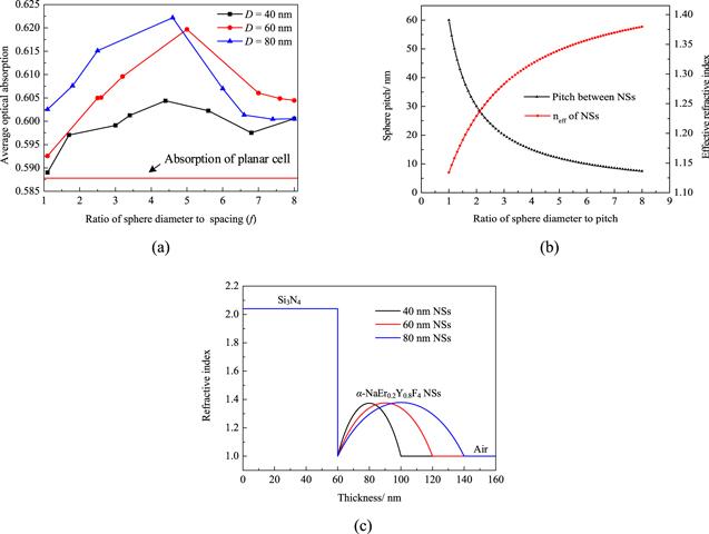
To investigate the effect of nanostructures on the surface of SCs, light-trapping properties of the planar SCs with different sizes of the α-NaEr0.2Y0.8F4 UC arrays on the surface were systematically studied. To get different f, the diameters of NSs were fixed and the pitch of NSs from large to small was swept. The relationship between average optical absorption of SCs and the change of ratio was plotted in figure 3. All other parameters used in this simulation were referred to in figure 1(a).
Figure 3.
 New window|Download| PPT slide
Figure 3.(a) The relationship between average optical absorption and the ratio of diameter to pitch. (b) The influence of the ratio of diameter to neff and NSs pitch. (c) Effective refractive indices of interfaces between air and SCs at the wavelength of 500 nm.
Figure 3(a) shows the influence of ratio change to average optical absorption of the SCs. The performance of SCs patterned with α-NaEr0.2Y0.8F4 NSs is obviously better than that of planar SCs with the same silicon thickness. From figure 3(a) we can see that when the ratio changes from 1 to 8, the average optical absorption of SCs with NS arrays on the surface increases at first, and then after a maximum peak appears the average optical absorption decreases. SCs patterned with larger NSs perform better in average optical absorption than the smaller ones. The highest average optical absorption and short circuit current density is gotten by SCs with NSs of D in 80 nm and f in 4.6, reaching to 62.22% and 27.23 mA cm−2, respectively. The results can be explained via the combined effect of the effective refractive index (neff) change on the surface and excitation of optical resonances [24, 25]. Referring to the effective medium theory, the high reflection originates from the mismatch between the refractive index of the air and SCs [26]. When the NSs are patterned on the surface of SCs, it will bring forth the gradient change of the refractive indices and ease the mismatch between the different materials [16], thus the reflection on the surface was reduced. Reducing the pitch between the NSs will change the filling ratio of nanostructure arrays, which has an effect on the neff of the interfaces between air and SCs [27]. The neff of NSs is got from calculation formula [27] at wavelength of 500 nm in 60 nm diameter NSs, shown in figure 3(b). In this wavelength the refractive indices of air and α- NaEr0.2Y0.8F4 can be seen as 1 and 1.5, while the refractive index of Si3N4 is 2.04. From figure 3(b) we can see that when the value of f is small, numerical variation has great influence on neff and sphere pitch. But after f increases to a certain degree, the influence of f changes on neff and sphere pitch decreases. Therefore, the absorption enhancement when f is between 1 and 5 in figure 3(a) is mainly due to the rapid increases of the neff of NSs, which enhances the gradient change of the refractive indices on the SCs surface, and significantly reduces the light reflection. However, when the pitch of the NSs is small enough, for the 60 nm NSs less than 10 nm, the α-NaEr0.2Y0.8F4 dielectric NSs can be seen as a layer of dielectric thin film [28]. Referring to Fresnel formula, the reflectivity can be derived from
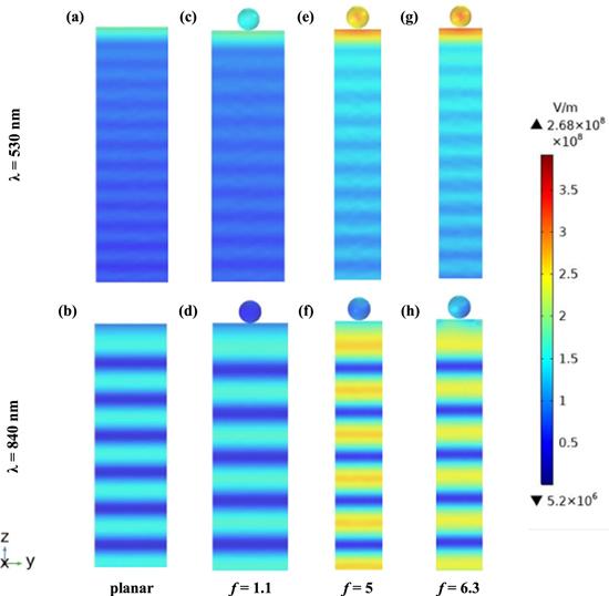
Figure 4 shows the comparison of electric field density between planar SCs and SCs patterned with α-NaEr0.2Y0.8F4 NSs on the surface.
Figure 4.
 New window|Download| PPT slide
Figure 4.The contours of the two-dimensional electric field intensity at 530 nm and 840 nm. (a), (b) Electric field intensity of planar SCs. (c) to (g) Electric field intensity of SCs with α-NaEr0.2Y0.8F4 NSs on the surface in ratio f=1.1, f=5 and f=6.3.
It can be found from figure 4(a) that most of the incident light cannot be absorbed by the silicon and the layered distribution of the electric field of the silicon layer is resulting from Fabry–Perot (FP) interference [29]. The profile of electric field intensity of SCs with α-NaEr0.2Y0.8F4 NS arrays on the surface are described in figures 4(c) to (h) and we can find that the incident light transmits better in figures 4(c) to (h) than the planar SCs. This is because there are more chances for light to enter the SCs after the sunlight bounces back and forth within the NSs and the electromagnetic wave energy is absorbed efficiently in silicon before the photons reach the bottom surface [30]. Comparing SCs with NSs on the surface in f=1.1 and f=6.3, stronger electric field distribution is observed within the SCs with NSs in f=5, thus leading to higher optical absorption. These phenomenon verify that too-sparse NSs have a disadvantage in light trapping and only moderately dense NSs can strongly strengthen the FP standing-wave resonance caused by the confinement light between the top surface and the back-reflector, which also ensures phase-matched coupling of an incident electromagnetic wave into a waveguide mode within the silicon [24]. In this case, the electric field intensity of SCs with the reasonable ratio of NSs arrays on the surface is relatively higher than that of others, which leads to a higher average optical absorption.
In total, the influence of α-NaEr0.2Y0.8F4 NSs to the average absorption of SCs are simulated in a sphere diameter ranging from 20 nm to 100 nm, which can be synthesized in the experiment at this stage [31]. Figure 5 draws the contour map of average optical absorption change due to the NS diameter and ratio change.
Figure 5.
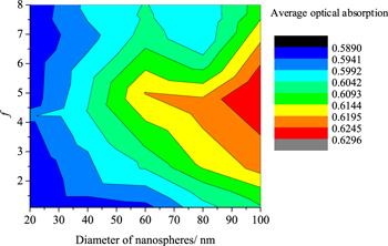 New window|Download| PPT slide
Figure 5.Contour map of average optical absorption when the α-NaEr0.2Y0.8F4 NSs diameter changes from 20 nm to 100 nm and ratio changes from 1 to 8.
As shown in figure 5, the average optical absorption of SCs varies with the changing of D and f. The best enhancement parameters focus on the D range from 60 to 100 nm and f range from 3.5 to 5.5. The highest average optical absorption is found to be at D=100 nm and f=5.2, reaching to 62.96% in average optical absorption and 27.32 mA cm−2 in Jsc, which is almost 8.5% enhancement than planar SCs with the same silicon thickness.
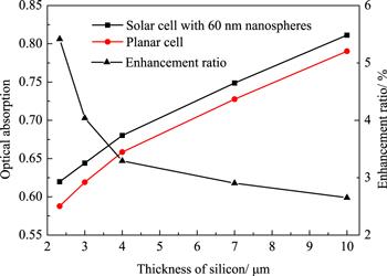
The average absorption enhancements of different thicknesses of silicon SCs with and without optimized structure were also calculated. The results are shown in figure 6.
Figure 6.
 New window|Download| PPT slide
Figure 6.Average absorption enhancement of different thickness (2330 nm, 3000 nm, 4000 nm, 7000 nm and 10 000 nm) of silicon SCs with and without 60 nm α-NaEr0.2Y0.8F4 NSs on the surface.
Figure 6 shows that with the increasing of silicon thickness, the average optical absorption of SCs with and without nanostructure on the surface are still increasing, reaching to 81.83% and 79.03% in 10 μm silicon thickness, respectively, showing that our structure still has the effect on thicker silicon. In contrast, the average optical absorption enhancement ratio of patterned SCs compared to planar SCs is slowly decreasing when the silicon becomes thicker. This result is mainly because the sunlight cannot enter the deep silicon with the increase of silicon thickness, which reduces the effect of surface nanostructure. The average optical absorption and Jsc enhancement of SCs in different silicon thicknesses are listed in table 1.
Table 1.
Table 1.The average optical absorption and Jsc enhancement in different types of silicon-based SCs.
| Si thickness (μm) | Average optical absorption (%) | Jsc (mA cm−2) | ||||
|---|---|---|---|---|---|---|
| Patterned | Planar | Enhancement | Patterned | Planar | Enhancement | |
| 2.33 | 61.97 | 58.78 | 5.42 | 27.04 | 25.75 | 5.02 |
| 3 | 64.41 | 61.91 | 4.04 | 27.99 | 27.08 | 3.37 |
| 4 | 68.02 | 65.85 | 3.29 | 29.52 | 28.54 | 3.42 |
| 7 | 74.88 | 72.77 | 2.91 | 32.71 | 31.77 | 2.97 |
| 10 | 81.13 | 79.03 | 2.65 | 35.21 | 34.33 | 2.56 |
New window|CSV
From table 1, we can find that the SCs with NSs on the surface achieve better performance than the planar SCs. Silicon SCs patterned with α-NaEr0.2Y0.8F4 NSs on the surface can prove significant in improving absorption and reducing reflection whose average optical absorption reaches 61.97% in a 2.33 μm silicon substrate and 81.13% in a 10 μm silicon substrate, respectively, increasing 5.4% and 2.7% compared to planar SCs with the same silicon thickness. The short circuit current densities of the two structures are about 27.04 mA cm−2 and 35.21 mA cm−2, respectively, which are also superior to the planar silicon SCs.
4. Conclusion
In general, numerical simulations of ultrathin silicon SCs with α-NaEr0.2Y0.8F4 NSs arrays on the surface were investigated. Our research shows that the closed packed α-NaEr0.2Y0.8F4 NSs have better light trapping performance than that of planar SCs. The highest average optical absorption was gotten by the SCs with α-NaEr0.2Y0.8F4 NSs on the surface are 100 nm in diameter and 5.2 in ratio. The SCs of 2.33 μm thick silicon substrate with NSs can achieve a short circuit current density of 27.32 mA cm−2 and a maximum optical absorption of 62.96%. This absorption accounts for 8.5% enhancement in comparison with the planar SCs with the same thickness of silicon in the wavelength ranging from 300 to 1150 nm. Considering the frequency UC of α-NaEr0.2Y0.8F4 NSs, this result would be much higher. Our work can guide the design and fabrication of α-NaEr0.2Y0.8F4 NSs arrays for enhancing the light management of crystalline silicon SCs. Further works are expected concerning the frequency UC of sodium yttrium fluoride materials, which may lead to the better performance of SCs.Acknowledgments
The numerical calculations in this paper have been done on the supercomputing system in the High Performance Computing Center of Yanshan University. The project was supported by the National Defense Science and Technology Innovation Special Zone, the Training Programme Fund for Talents of Hebei Province (A201902010), the Natural Science Fund of Hebei Province (F2018203263), the Educational Commission of Hebei Province (ZD2016054), Graduate innovative funding program of Hebei Province (CXZZBS2018057).Reference By original order
By published year
By cited within times
By Impact factor
DOI:10.1002/pip.2371 [Cited within: 1]
DOI:10.1016/j.solmat.2016.06.014 [Cited within: 1]
DOI:10.1021/ja910082y [Cited within: 1]
DOI:10.1016/j.optcom.2019.07.038 [Cited within: 1]
DOI:10.1038/srep22136 [Cited within: 1]
DOI:10.1155/2015/561586 [Cited within: 1]
DOI:10.1016/j.nanoen.2014.03.004 [Cited within: 1]
DOI:10.1063/1.3687352 [Cited within: 1]
DOI:10.1016/j.solmat.2005.09.021 [Cited within: 1]
DOI:10.1063/1.1654325 [Cited within: 1]
DOI:10.1038/srep29871 [Cited within: 1]
DOI:10.1002/adma.201000488 [Cited within: 1]
DOI:10.1021/nl9034237 [Cited within: 1]
DOI:10.1002/anie.201600702 [Cited within: 1]
DOI:10.1039/c7nr01008g [Cited within: 1]
DOI:10.1016/j.optcom.2016.05.050 [Cited within: 2]
DOI:10.1186/1556-276X-9-73 [Cited within: 1]
DOI:10.1016/j.jqsrt.2013.09.021 [Cited within: 1]
DOI:10.1364/OE.22.0000A1 [Cited within: 1]
DOI:10.1103/PhysRevB.3.262 [Cited within: 1]
DOI:10.1103/PhysRevA.1.513 [Cited within: 1]
DOI:10.1016/j.jlumin.2018.07.042 [Cited within: 1]
DOI:10.1002/adma.201004393 [Cited within: 1]
DOI:10.1038/srep30503 [Cited within: 2]
DOI:10.1038/nmat3921 [Cited within: 2]
DOI:10.1002/adfm.201201949 [Cited within: 1]
DOI:10.1063/1.3650266 [Cited within: 2]
DOI:10.1364/OL.38.003057 [Cited within: 1]
DOI:10.1016/j.optcom.2015.08.069 [Cited within: 1]
DOI:10.1063/1.3633119 [Cited within: 1]
DOI:10.1021/cr400425h [Cited within: 1]
