 ,1,?, Lei Sun1, Guo-Rong Zhang2, Can Deng1, Yi-Teng Tu2, Li Guan3
 Corresponding authors: ? E-mail:tanxin@ctgu.edu.cn
Received:2019-06-1Online:2019-11-1
| Fund supported: |

Abstract
Keywords:
PDF (7181KB)MetadataMetricsRelated articlesExportEndNote|Ris|BibtexFavorite
Cite this article
Xin-Yu Tan, Lei Sun, Guo-Rong Zhang, Can Deng, Yi-Teng Tu, Li Guan. Absorption Enhancement of Ultrathin Crystalline Silicon Solar Cells with Dielectric Si3N4 Nanostructures *. [J], 2019, 71(11): 1346-1352 doi:10.1088/0253-6102/71/11/1346
1 Introduction
Since the beginning of the 21st century, people are increasingly looking forward to the era of solar power generation under the serious impact of the two major crises of bottoming out of oil exploitation and deteriorating since ecological environment.[1] Solar energy is an inexhaustible source of renewable energy for mankind, which does not generate any environmental pollution. Photovoltaic is one of the fastest growing fields of research in recent years.[2] To this end, people developed solar cells. There are many types of solar cells, such as crystalline silicon solar cell, amorphous silicon solar cell, GaAs Solar Cells and Perovskite solar cells, etc. Silicon solar cells play a very important role in the photovoltaic industry.[3] Crystalline silicon solar cells occupy the dominant position in the solar cell market. Its preparation technology represents the preparation technology of the entire photovoltaic cell industry. Traditional crystalline silicon solar cells consist of silicon, the main part of the solar cell is fragile and easy to produce invisible cracks. Most of them have a layer of toughened glass as protection, resulting in heavy weight, inconvenient portability, poor seismic capacity, high cost. Thin film solar cells overcome the above shortcomings but with lower efficiency. Thin film silicon solar cells become increasingly important because high efficiency and low manufacturing costs of photovoltaic cells both need to be taken into account at the same time. Light trapping is a vital factor in the development of thin-film photovoltaic devices. Cell performances reduce with the active layers becoming thinner. One approach to enhancing their light utilization efficiency is to reduce the reflection of the incident light by front surface modifications. Until now, a number of proposals have been taken to achieve the goal, including anti-reflective coating and surface texturing. First method is to reduce the reflection on front surface. Second method increases the optical path length of light within the cell. For the former sort, reducing reflection on the surface via introducing the quarter wavelength antireflection layer has been proposed. Certain intermediate materials are usually used, such as silicon dioxide (SiO$_{2}$),[4] silicon nitride (Si$_{3}$N$_{4} $),[5-6] and other transparent conductive oxides.[7] The second category is to construct surface texture ranging from random arrays to regularly arrays for more lights scattering or gain light scattering from noble metal nanoparticles that are excited at their surface plasmon resonance. The scattering may availably enhance the light absorption in thin film solar cells. For the first method, different materials have been studied for simulated results show that, an individual antireflection film in solar cells at the beginning. Then multiple antireflection films also have been investigated. As for the second method, a great number of nanostructures or metal nanoparticles[8-11] were proposed to increase light absorption, such as constructing photosensitive materials into arrays like nanoparticles,[11] nanowires,[12-15] nanoholes (NHs),[16-22] nanocones (NCs)[23] or introducing surface plasmons. Later combination methods show better results have been proposed,[24-26] In most of the articles, the researchers used the experience of predecessors to construct the surface morphology (make more light reflection happen) directly on solar cell material or to add multiple anti-reflection layers (make more light enter the cell) on the material. In this article, we combine two approaches to adding a textured anti-reflection layer on the surface of a solar cell to make both light reflection and anti-reflection happen at the same time and further produce optical coupling. The structure can be easily achieved by using nano-imprint lithography.[27] We systematically studied how the depth of circular truncated cone holes (CTCs), antireflection layer's thickness, duty circle, thickness of silver and period affects solar cell's short-current current density ($J_{\rm sc}$) character. Simulated results show that a $J_{\rm sc}$ of 30.17 mA/cm$^{2}$ was produced in optimum parameters at an equivalent thickness of 2330 nm, produces an short-circuit current enhancement of 32.44% with respect to the planar reference system in the range of 300 nm to 1100 nm. And with a silver rear reflection equipped, the $J_{\rm sc}$ and short-circuit current enhancement mentioned above can be achieved to 32.26 mA/cm$^{2}$.2 Methods
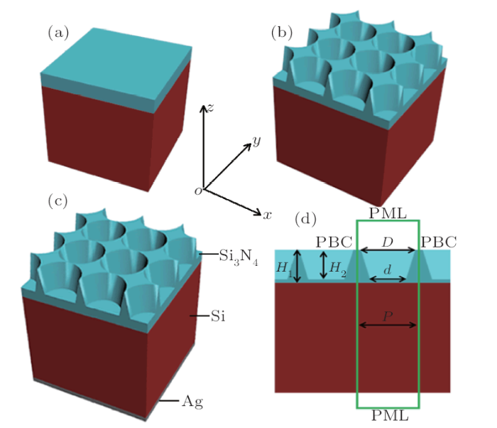
3D diagram of the control group shows in Fig. 1(a). It is a solar cell with 67 nm flat ${\rm Si_{3}N_{4}}$ anti-reflection layer.[33] We choose this thickness of ${\rm Si_{3}N_{4}}$ as control group because it has already been optimized and confirmed in Ref. [33]. Figure 1(b) displays the diagram of designed cells with ${\rm Si_{3}N_{4}}$ CTCs etched by air. Model in Fig. 1(c) adds a rear reflection layer compared with the model in Fig. 1(b). The geometric parameters were introduced in Fig. 1(d). The period of the model is shown as $P$. The thickness of ${\rm Si_{3}N_{4}}$ layer is set as $H_{1}$, and the depth of CTCs is set as $H_{2}$. The thickness between hole and silicon is $H_{3}$. The relationship between $H_{1}$, $H_{2}$, and $H_{3}$ is defined as $H_{1}=H_{2}+H_{3}$. The diameter on the top of CTCs is $D$. The diameter on the bottom of CTCs is $d$. The top duty circle ($t_{\rm dc}$) and bottom duty circle ($b_{\rm dc}$) of nanostructures is defined as $t_{\rm dc}=D/P$ and ${b}_{\rm dc}={d}/{P}$,[28] respectively. In our work, the thickness of active layer is fixed as 2.33 um for Refs. [19, 21$-$22]. All outcomes gained by data simulation were calculated via finite difference time domain (FDTD) method. Many different numerical methods have been used to calculate absorptivity of solar cells such as transfer matrix method (TMM),[12] finite-difference time-domain method (FDTD),[10,17] rigorous coupled-wave analysis (RCWA)[22] and finite element method (FEM).[11] Compared with other numerical methods, the FDTD can be easy to calculate the distribution of electromagnetic field of arbitrary material and structure. So FDTD method is employed to simulate the optical behaviors of nanostructures in this paper. In our paper, we simulated a plane wave in the range of (300--1100) nm as incident light. The boundary conditions in $x$-direction and $y$-direction are set to periodic. The boundary condition in $z$-direction is set to PML (Perfect Match Layer). The optical constants for all the media studied in this work were provided in Palik's experimental data.[29] The p-type and n-type regions are deemed to be slightly doped so they can be modelled by identical optical constants as intrinsic crystalline silicon. In our simulations, front reflectance $R(\lambda)$ on the surface and the transmittance $T(\lambda)$ at the back surface were measured, and the absorptance was defined by $A(\lambda)=1-R(\lambda)-T(\lambda)$. Supposing every electron-hole pair benefits photocurrent, the short-circuit current density ($J_{\rm sc}$) is gained by:[30]Fig. 1
 New window|Download| PPT slide
Fig. 1(Color online) (a) 3D diagram of structure with 67 nm flat Si$_{3}$N$_{4}$ used as a control group for optimization of texture parameter using simulation. (b) 3D diagram of structure with Si$_{3}$N$_{4}$ CTCs arrays used for optimization of texture parameter using simulation. (c) 3D diagram of structure with Si$_{3}$N$_{4}$ CTCs arrays and back silver reflector used for optimization of texture parameter using simulation. (d) Schematic of the FDTD simulation model in
where, e means the charge of an electron, $c$ means the speed of light in the free space, $h$ means Plank's constant,$\lambda_g$ means the free space wavelength corresponding to the band gap of c-Si ($g E = 1.12$ eV), i.e. 1127 nm, and $I_{{\rm AM}1.5}(\lambda)$ is the solar irradiance under the global 37$^{\circ}$ tilt Air Mass 1.5 spectrum.[31]
3 Results and Discussion
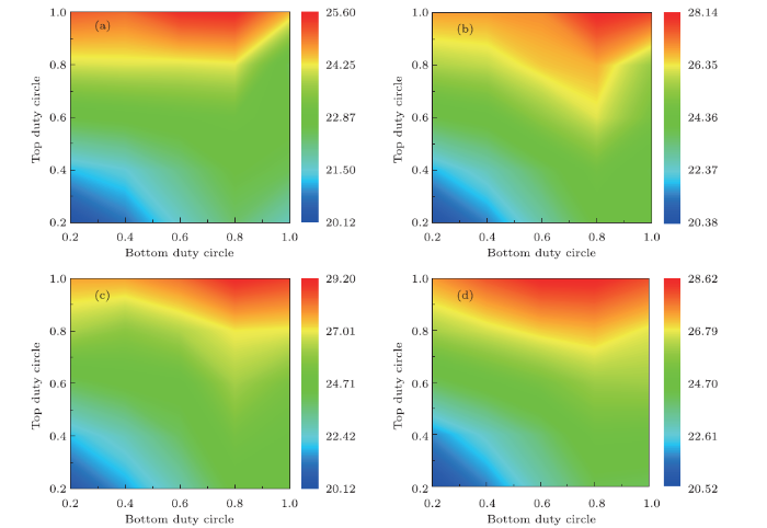
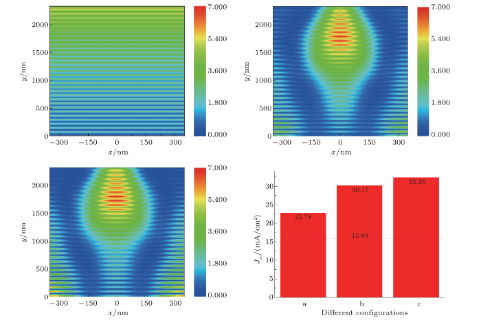
In order to compare and explain the validity of the approach, we first studied the $J_{\rm sc}$ of 2330 nm bare c-Si film and the optimized structure only equipped with a 67 nm flat ${\rm Si_{3}N_{4}}$ antireflection as control group. The $J_{\rm sc}$ of 2330 nm bare c-Si film is 15.89 mA/cm$^{2}$ calculated via the formula. And the $J_{\rm sc}$ of control group is $J_{\rm sc}$ = 22.78 mA/cm$^{2}$. Figure 2 shows the relationship between $t_{\rm dc}$ and $b_{\rm dc}$ in different period. The ${t}_{\rm dc}$ and ${b}_{\rm dc}$ are studied for different array period values $P$ that ranging from 500 nm to 800 nm in steps of 100 nm while ${t}_{\rm dc}$ and ${b}_{\rm dc}$ are both set varying from 0.2 to 1.0 in steps of 0.2. ${H}_{1}$ is first set as 500 nm and ${H}_{2}$ is first set as 450 nm. We use two-dimensional sweeping to find the best value of ${J}_{\rm sc}$ in order to find the best ${t}_{\rm dc}$ and ${b}_{\rm dc}$. Based on this we can find the best period from the trend of ${J}_{\rm sc}$ as the period raising.Fig. 2
 New window|Download| PPT slide
Fig. 2(Color online) Relationship of ${J}_{\rm sc}$ under different combinations of $t_{\text{dc}}$ and $b_{\text{dc}}$ in different period. (a) ${P} = 500$ nm, (b) ${P} = 600$ nm, (c) ${P} = 700$ nm, (d) ${P} = 800$ nm.
We can learn from Figs. 2(a)--2(d) that at the same period, there is a region of high ${J}_{\rm sc}$ where the ${b}_{\rm dc}$ ranges from 0.2 to 1.0, ${t}_{\rm dc}$ values 1.0. This shows that ${J}_{\rm sc}$ rises with increasing size of the circular truncated cone top hole. We can see that the results of ${J}_{\rm sc}$ reach to the peak when ${t}_{\rm dc}$ and ${b}_{\rm dc}$ are set as 1.0 and 0.8, respectively. The ${J}_{\rm sc}$ increases from 500 nm to 700 nm in period but decreases in 800 nm. The drop at 800 nm indicates that the textured ${\rm Si_{3}N_{4}}$ has the best matching light absorption coupling effect when adjusting the duty circle of the circular truncated cone holes at a period of 700 nm. So the period is fixed in 700 nm. The peak value of ${J}_{\rm sc}$ is 29.20 mA/cm$^{2}$, produces a short-circuit enhancement of 28.18% with respect to the reference planar system.
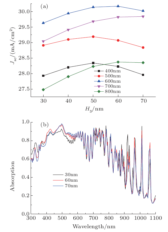
Next, we try to find the influence of ${H}_{1}$ and ${H}_{3}$ on ${J}_{\rm sc}$. In Fig. 3(a), here ${t}_{\rm dc}$ and ${b}_{\rm dc}$ are fixed as 1.0 and 0.8. And period is fixed in 700 nm based on above results. From Fig. 3(a) we can see that ${J}_{\rm sc}$ increased initially, followed by a decrease and the best result shows when ${H}_{3}$ is 50 nm at the same time ${H}_{1}$ ranges from 400 nm to 500 nm. When ${H}_{1}$ reaches 600 nm, the peak of ${J}_{\rm sc}$ approaches when ${H}_{3}$ is 60 nm because of a combination effect caused by our designed structure. And ${J}_{\rm sc}$ decreases absorption occurs obviously when ${H}_{1}$ ranges from 700 nm to 800 nm. And the best choice of ${H}_{1}$ and ${H}_{3}$ is 600 nm and 60 nm, respectively. The best value of ${J}_{\rm sc}$ is 30.17 mA/cm$^{2}$, generates a short-circuit enhancement of 32.44%. We can roughly see the relationship between ${H}_{3}$ and absorption of silicon in Fig. 3(b). With the increasing of ${H}_{3}$, the absorption increases as ${H}_{3}$ raises in the range of 450 nm to 590 nm, which is in accord with the theory of quarter wavelength layers. The ${\rm Si_{3}N_{4}}$ thin film between hole and silicon acts as a single quarter wavelength layer, which enhances the absorption in this area. But the absorption decreases as ${H}_{3}$ raises before 450 nm, The absorption before 450 nm decreases significantly when ${H}_{3}$ increases to 70 nm, which makes the best total absorption occur if ${H}_{3}$ is set as 60 nm.
Fig. 3
 New window|Download| PPT slide
Fig. 3(Color online) (a) Relationship between ${J}_{\rm sc}$ and ${H}_{3}$ at different ${H}_{1}$. (b). Absorption spectrum for Si with different ${H}_{3}$. (40 nm, 50 nm not shown here because the lines are too dense).
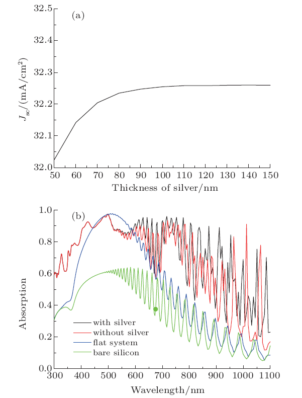
The front system plays an important role in weakening the front reflection. After determining the best parameters on the front system of silicon, a rear reflector to enhance the back reflection is designed and studied to understand the behavior of the CTCs arrays. In order to enhance back reabsorption, a thin silver layer is designed to the back. The thickness of a flat silver back reflection (${H}$) is been swept and shown in Fig. 4(a). From Fig. 4(a) we can see that, when thickness of silver ranges from 50 nm to 110 nm, the ${J}_{\rm sc}$ increases slowly. When ${H}$ is above 110 nm, the ${J}_{\rm sc}$ shows no increasing. So the optimized ${H}$ we chose as 110 nm. Comparison of absorption spectra for different configurations lists in Fig. 4(b). From Fig. 4(b) we can see that, the absorption curve with the front system has greatly improved below the 450 nm compared with the flat system absorption curve. This is because that this wavelength band cannot enter the deep silicon. And the optical path is increased due to the combined effects of diffraction, reflection and refraction when the light enters the front system. In the wavelength range of 500 nm--590 nm, the comparison of the light absorption curves shows that the silicon absorption with the front system is slightly inferior to that of the quarter-wavelength layer specially constructed to enhance absorption in this band. The flat system absorption curve at a wavelength greater than 590 nm exhibits a well-shaped Fabry-Perot resonance. In the wavelength below 500 nm areas, light does not reach to the silver layer so the absorption curve with or without silver is the same.
Fig. 4
 New window|Download| PPT slide
Fig. 4(Color online) (a) Relationship between ${J}_{\rm sc}$ and thickness of back silver. (b) Comparison of absorption spectra for different configurations. Blue line means the absorption spectrum equipped with 67 nm flat ${\rm Si_{3}N_{4}}$. Red line means the absorption spectrum only with front system. Black line means the absorption spectrum with front system and back flat silver reflector. Green line means the absorption spectrum of bare silicon.
In the wavelength above 500 nm areas,light reaches the bottom of the silver layer and being reabsorbed. It leads to a peak Jsc reaches 32.26 mA/cm$^{2}$. The reference cell is an anti-reflection layer constructed in accordance with a quarter-wavelength layer that enhances transmission in the corresponding wavelength region to enhance absorption. After the morphology is formed, light absorption is a combined effect of anti-reflection and grating. An unusual light absorption decreasing occurred because of partly destructive interference (such as in the wavelength region of (500--600) nm). So light absorption in this area is weakened. But it should be noted that in the entire wavelength range except for (500--600) nm, our structure undoubtedly enhances light absorption.
To comprehend the optical behaviors in silicon layer, we compared the outcome of the control group, structure with ${\rm Si_{3}N_{4}}$ CTCs arrays and structure with ${\rm Si_{3}N_{4}}$ CTCs arrays and back silver reflector. The absorption per unit volume, normalized to source power, can be calculated. Figure 5 shows the profile of the optical absorption per unit volume.[21] The unit is watt/um$^{3}$. The absorption density maps of x-z cross-section are shown in Figs. 5(a)--5(c) at the wavelengths of 600 nm. Figures 5(a)$-$5(c) display the absorption density maps of silicon in the structures configured as showed in Figs. 1(a)--1(c), respectively. It can be seen from the wave pattern of the light absorption field that the light resonates strongly in the structure. Compared to the control group, structure with ${\rm Si_{3}N_{4}}$ CTCs arrays make more incident light enter deeper silicon. Thus, the absorption has been greatly improved. And structure with ${\rm Si_{3}N_{4}}$ CTCs arrays and back silver reflector further enhance the bottom absorption (Fig. 5(c)). It can be known from Fig. 5(d) that the front ${\rm Si_{3}N_{4}}$ CTCs arrays provide a great positive impact on light absorption. With a back reflector equipped, the absorption can be further improved.
Fig. 5
 New window|Download| PPT slide
Fig. 5(Color online) Two-dimensional light absorption density distribution profiles of the silicon part in our solar cell at a wavelength of 600 nm of $x$-$z$ cross-section. (a) The structure of control group corresponds to
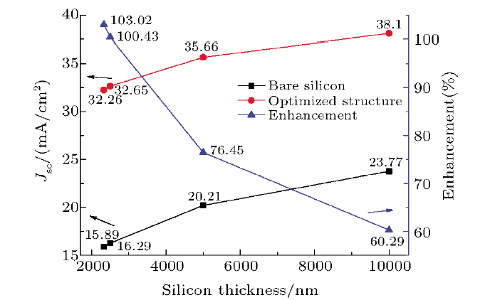
Later the ${J}_{\rm sc}$ enhancements of different thickness of silicon solar cells with and without optimized structure were calculated. The results are shown in Fig. 6. The results show that with the increase of silicon thickness, the solar cell ${J}_{\rm sc}$ equipped with our optimized structure is still strengthening, but this enhancement is slowly decreasing due to the increase of silicon thickness. This is because the sunlight cannot enter the deep silicon with the increasing of silicon thickness. At the same time, this also shows that our structure does have the effect of enhancing light absorption. Nevertheless, in reality, effects such as drift-diffusion and uncertainties will continue to appear in real solar cells. Therefore, the ${J}_{\rm sc}$ obtained in reality will not reach the theoretical consequences. So far, thickness of 2330 nm silicon has become a research hot spot for many researchers. Compared to structures with absorbent layers of the same thickness, the short circuit photocurrent density approached by our structure is greater than the majority of the reported outcome.[19, 21] In order to better compare the final results, we change the thickness of silicon to 2 um. A 30.37 mA/cm$^{2}$ ${J}_{\rm sc}$ could be generated and the outcome is also better than the result achieved by the structure with front-grating in Ref. [32]. The Yablonovitch limit of 2 um silicon can generate a short circuit current of 35.5 mA/cm$^{2}$. Compared to structure in Ref. [23], our ${J}_{\rm sc}$ is lower. But our structure is not modified in the structure of silicon.
Fig. 6
 New window|Download| PPT slide
Fig. 6(Color online) ${J}_{\rm sc}$ enhancement of different thickness (2330 nm, 2500 nm, 5000 nm, 10000 nm) of silicon solar cell with and without optimized structure.
It is a modification of the structure of silicon nitride, and technically our structure forming technology is well developed. From this point of view, our structure is still innovative. We studied the enhancement of light absorption by front textured anti-reflection film combined with simple back single-layer reflective layer. From the perspective of optical research, a stronger enhancement was obtained by adding a front strong light trapping structure and a back strong reflection structure. This is a trend in the field of lighting trapping structures, which we will further design in our future research.
4 Conclusion
In general, the investigations on ultrathin-film silicon solar cells are necessary due to a variety of motivations. The effect of setting up a texture of antireflection layer on ability of light trapping was methodically studied and it can help to achieve higher photocurrent density for the improved PCE. We proposed and investigated ultrathin silicon solar cell architecture with CTCs anti-reflection layer. In CTCs, the available light bounces repeatedly in the hole and couples into silicon. And the thin-film ${\rm Si_{3}N_{4}}$ under the hole also has a positive influence on the enhancement of the couple. The combined effect of these two aspects produces a better ${J}_{\rm sc}$. The results indicate that cells with ${\rm Si_{3}N_{4}}$ CTCs arrays get a stronger ability to absorb the light. The ${J}_{\rm sc}$ generated by the cells with ${\rm Si_{3}N_{4}}$ CTCs arrays reaches 30.17 mA/cm$^{2}$, which is 32.44% higher than the value gained by control group. And by simply adding a layer of silver rear reflection to the optimized configuration above, brings a photocurrent of 32.26 mA/cm$^{2}$, produces a best short-circuit current enhancement of 41.62% higher than the control group. Although ${\rm Si_{3}N_{4}}$ is an insulator, the CTCs of our structure owns a great space. Thickness between Si3N4 and silicon is only 60 nm. The planar silicon solar cell on the market can be achieved in a thickness of 75 nm ${\rm Si_{3}N_{4}}$. So this will not be a problem for preparation. In summary, the calculations presented in this paper demonstrate that it is potential to enhance absorption by building textures on antireflection layers.Reference By original order
By published year
By cited within times
By Impact factor
[Cited within: 1]
[Cited within: 1]
[Cited within: 1]
[Cited within: 1]
[Cited within: 1]
[Cited within: 1]
[Cited within: 1]
[Cited within: 1]
[Cited within: 1]
[Cited within: 3]
[Cited within: 2]
[Cited within: 1]
[Cited within: 1]
[Cited within: 1]
[Cited within: 1]
[Cited within: 2]
[Cited within: 2]
[Cited within: 2]
[Cited within: 1]
[Cited within: 1]
[Cited within: 1]
[Cited within: 1]
[Cited within: 1]
[Cited within: 1]
URL [Cited within: 1]
[Cited within: 1]
[Cited within: 2]
