Shuang Shuang1, Zheng Xie1,2,Zhengjun Zhang3
(1. State Key Laboratory of New Ceramics and Fine Processing, School of Materials Science and Engineering, Tsinghua University, Beijing 100084, China; 2.High-Tech Institute of XiˇŻan, XiˇŻan 710025, China; 3.Key Laboratory of Advanced Materials (MOE), School of Materials Science and Engineering, Tsinghua University, Beijing 100084, China)
Abstract:
The glancing angle deposition (GLAD) method is a kind of physical vapor deposition and many kinds of self-standing nanostructured materials can be prepared. Here we report GLAD method to form self-standing TiO2 nanostructures on specific substrates, which makes photocatalysts easier to recycle. And smart designs of doping, decorating band gap matched materials can also make traditional photocatalysts take use of more visible light. In this review, we present some previous work fabricating nanostructured TiO2 composites for enhanced photocatalytic performance by these methods.
Key words: glancing angle deposition TiO2 photocatalytic nanostructure
DOIŁş10.11916/j.issn.1005-9113.17037
Clc Number:X703
Fund:
Shuang Shuang, Zheng Xie, Zhengjun Zhang. Review:Nanostructured TiO2 for Enhanced Photocatalytic Property by Glancing Angle Deposition Method[J]. Journal of Harbin Institute of Technology, 2017, 24(5): 1-11. DOI: 10.11916/j.issn.1005-9113.17037.

Fund Sponsored by the Ministry of Science and Technology of P.R.C(Grant No. 2016YFE0104000) Corresponding author Zhengjun Zhang, Winner of the Ministry of Education of Yangtze River Scholar Professor. E-mail: zjzhang@tsinghua.edu.cn. Article history Received: 2017-03-07
Contents Abstract Full text Figures/Tables PDF
Review:Nanostructured TiO2 for Enhanced Photocatalytic Property by Glancing Angle Deposition Method
Shuang Shuang1, Zheng Xie1,2, Zhengjun Zhang3


1. State Key Laboratory of New Ceramics and Fine Processing, School of Materials Science and Engineering, Tsinghua University, Beijing 100084, China;
2. High-Tech Institute of Xi'an, Xi'an 710025, China;
3. Key Laboratory of Advanced Materials (MOE), School of Materials Science and Engineering, Tsinghua University, Beijing 100084, China
Received: 2017-03-07
Fund: Sponsored by the Ministry of Science and Technology of P.R.C(Grant No. 2016YFE0104000)
Corresponding author: Zhengjun Zhang, Winner of the Ministry of Education of Yangtze River Scholar Professor. E-mail: zjzhang@tsinghua.edu.cn.
Abstract: The glancing angle deposition (GLAD) method is a kind of physical vapor deposition and many kinds of self-standing nanostructured materials can be prepared. Here we report GLAD method to form self-standing TiO2 nanostructures on specific substrates, which makes photocatalysts easier to recycle. And smart designs of doping, decorating band gap matched materials can also make traditional photocatalysts take use of more visible light. In this review, we present some previous work fabricating nanostructured TiO2 composites for enhanced photocatalytic performance by these methods.
Key words: glancing angle deposition TiO2 photocatalytic nanostructure
1 IntroductionWith the rapid industrial development and population growth, serious environment and energy crisis have been increasingly severe. Hence people make every efforts to solve these problem[1-3]. Sufficient utilization of solar energy can be one solution to alleviate energy issues. Photocatalysts especially semiconductors could exchange chemical energy from light irradiation. They can be good choices to decompose organic pollutants, which have drawn huge interests of researchers[4-7].
There are plenty of ways to fabricate nanostructure materials from previous research. And glancing angle deposition (GLAD) is a highly repeatable method to achieve large area 1-Dimension and 2-Dimension nanomaterials. The principle is to utilize adatom diffusion and atomic shadowing. The e-beam deposition system is shown in Fig. 1. And the porous films are fabricated by mounting the specific substrate face to vapor flux. During deposition, the angle of incidence and rotation can be controlled independently then it can change the porosity and rod direction of the film[8-14].
Figure 1
 Figure 1 Electron beam evaporator with oblique angle deposition configuration, with 2-axis control of the orientation of the substrate with the vapor[8]
 Until now, there has been many kinds of materials prepared via GLAD method for photocatalysts. Pradip Basnet et al.[15] have fabricated CuxO (x=1, 2) nanorod arrays (NRAs) through annealing Cu NRs fabricated by GLAD. By simply changing the thermal oxidation temperature, they can control the composite of Cu2O, CuO, or mixed phase Cu2O/CuO polycrystalline[15]. This group also achieved the preparation of ¦Á-Fe2O3 Nanocolumns (NCs) and NRs by GLAD method. And they found that the reduced rates of NRs were not a monotonic function with heat treatment parameters[16]. And morphology like such as zigzag[17-20], spirals[21-24], slanted posts columns[25-27], nanopillars[28-32] can all be synthesed. A kind of special shape will be utilized in numerous application.
Since 1972 Fujisima and Honda[33] found photocatalytic splitting phenomenon over water through TiO2 photoanode. Because of its environment friendly property, chemical inertness, photostability and wide existence[34-35], TiO2 has been considered as one of the superior photocatalyst and until now it still has been broadly studied to handle the environmental concerns. But wide band gap (~3.2 eV) leads it can only absorb ultraviolet (UV) light occupying ~5% in sunlight energy[36]. The strategies to improve performance can be divided to three main ways: 1) coupling with band gap matched oxidize or sulfide (e.g., TiO2/Cu2O[37] and TiO2/WO3[38]); 2) decoration of SERS effect metals (e.g., Au/TiO2[39], Pt/TiO2[40] and Ag/TiO2[41-42]); 3) doping other element atoms (e.g., oxygen defects[43], and sulfur[44], nitrogen[45]).
2 Doping Non-metal and Metal IonDoping non-metal ion is a common way to change the band gap of TiO2. Especially, the response wavelength range of TiO2 can be shifted from UV to visible light largely but it will also hinder its photo-catalytic activity. And now non-metal ion such as nitrogen[46], sulphur[47], and fluoride[48], has been considered as main solution to eliminate the corruption of the thermal stability. Since Asahi et al.[49] studied that N-doping into TiO2 could narrow down the band gap and improved the photocatalytic property under visible light.
By using GLAD method, Xie et al.[50] deposited TiN NRAs by liquid nitrogen. Furthermore they oxided TiN NRAs in air at 330 ˇć, and changed annealing time to have various N contents (from 5 min to 120 min). And samples were named as different time.
2.1 TiO2 NRAs with Nitrogen Element DopedThe TiN NRAs were fabricated by GLAD method through liquid nitrogen. Then we oxided the as-prepared TiN NRAs into N-doped TiO2 NRAs by heating in air at 330 ˇć. The scanning electron microscope (SEM) images for all samples were shown in Fig. 2. The cross sectional surface of NRs was shown in the inset of Fig. 2(a) which length is around 600 nm uniformly. And the morphologies with different annealing time do not vary largely and they are correspondingly exhibited in Figs. 2(b)-(f).
Figure 2
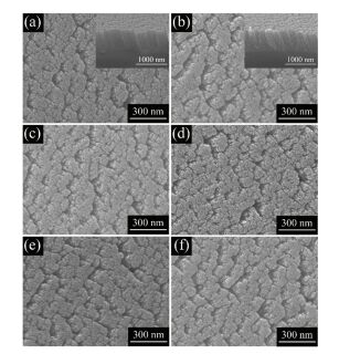 Figure 2 SEM images of (a)TiN NRAs and as-prepared sample annealing for (b) 5 min, (c)15 min, (d)30 min, (e)60 min, (f) and 120 min[50]
 In order to study microstructures of all samples in detail, transmission electron microscope (TEM) is also shown in Fig. 3. Herein Fig. 3(a) shows that all NRs show both similar size, including ~600 nm in length and ~80 nm in diameter, compared with SEM results. The high-resolution TEM (HRTEM) image of samples is presented in Fig. 3(b). We can see the TiN crystalline grains clearly especially the (200) plane corresponding to 0.212 nm interplanar spacing. Thus, TiN could be oxidized into TiO2 completely in air at medium temperature. Furthermore, the annealing time can also be a key to change the final oxidation degree. The most part of sample named 15 minN-TiO2 NRAs is amorphous state. And a small part of crystalline grains also exists with 0.354 nm lattice spacing in Fig. 3(c). With the prolonging of annealing treatment time, crystalline degree of TiO2 shows more and more from Fig. 3(d).
Figure 3
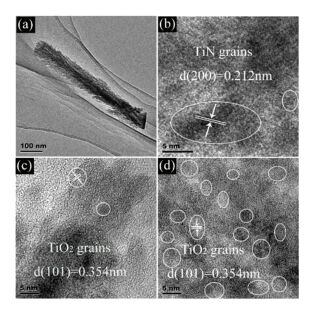 Figure 3 TEM and HRTEM images of TiN NRAs(a) (b); samples annealing for 5 and 120 min (c) (d)[50]
 Fig. 4(a) shows the UV-visible light transmittance spectra of the all samples. We can see from figures that the transmittance value between 300 and 600 nm increases with prolonging time of annealing. According to previous research, people can use the absorption coefficient to calculate the optical gap (Eg) ¦Á, if scattering effect is neglected, they can be below:
Figure 4
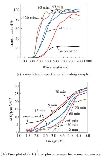 Figure 4 Transmittance spectra and Tauc plot of (¦ÁE)1/2 vs photon energy for annealing sample[50]
 (¦ÁEg)n=A(Eg-¦Ç¦Ô)
Here the indirect transmission n is 1/2[51]. What's more, Fig. 4(b) also shows the Tauc plot of (¦ÁE)1/2 changes with various photon energy (E=h¦Í). Band gap could be obtained through extending linear to (¦ÁE)1/2=0. Here 120 minN-TiO2 NRAs owns band gap about 3.19 eV quite closed to pure anatase. This result shows that the TiN is totally translated into TiO2 through oxidizing.
2.2 Nb-doped TiO2 NRAsTucker et al.[52] have fabricated a range of NbxTi1-xO2 compositions through electron beam evaporation. And they studied the effect of Nb content on Transparent conducting oxides properties in detail. Fig. 5 shows the transmission of representative films of as prepared film and some heat treatment samples. The spectra shows typical fringes also with decreasing transparency when they increased gas flow rate or annealing temperature. However, transparency changes little in the visible region for the different annealing conditions. What's more, transmissions at infrared wavelengths have varied much more. So free electrons became more and more with the decline of transmission when they change the annealing conditions.
Figure 5
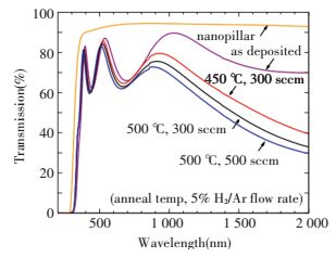 Figure 5 Optical transmission of all annealing samples[52]
 2.3 Sm-doped TiO2 NRAsXiao et al.[53] have tried to prepare 2% Sm3+ doped TiO2 thin films via GLAD method. Firstly, the stoichiometric amount of Sm2O3 was added into TiO2 powder. After mixing homogeneity, the round bulk with TiO2: 2mol% Sm3+ was pressed by tablet machine. The bulk was used as raw material for oblique angle electron beam deposition. After thin film prepared, they are heated at 600, 700, 800 ˇć for 2 h in atmosphere. Here the transmission value at 500 nm was also found increased from 8% to 33% with heat treatment. Besides, this kind of thin film with polarized PL also can be potentially used as some biology micro devices.
3 Coupling with Other SemiconductorSemiconductors own narrow band gap such as PbS[54], CdSe[55], ZnS[56], and CdS[57-58] can usually be combined with TiO2 to shift light response range. And among them, CdS (~2.4 eV) is a great candidate[59-60]. Specially nano sized TiO2 performs better behaviour on both reduction and recombining with photo-generated electrons[61].
3.1 Decorated CdS nanoparticles (NPs) on TiO2 NRAsXie et al.[62] have also fabricated CdS decorated TiO2 NRAs using GLAD technique. Firstly, Ti NRAs were first deposited. Then they were annealed by tube furnace of 450 ˇć for 2 h in air. CdS NPs were made by successive ion layer adsorption and reaction (SILAR) method[63]. The substrates were successively immersed in specific concentration of Na2S and Cd(Ac)2 solutions alternatively each for 30 s to let them react and gain CdS NPs. During the process, the substrate was also raised by DI water between each solution. Fig. 6(a) is the SEM image of Ti NRAs from top of view. We can see that Ti NRs were inclined on the substrate. And Figs. 6(b)-(f) are the SEM image of pure and original sample with various SILAR cycles decoration.
Figure 6
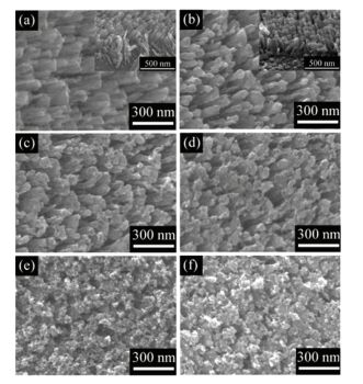 Figure 6 SEM pictures of (a) Ti NRAs; (b) TiO2 NRAs sample; (c-f) CdS decorated 5, 10, 15, 20 cycles[62]
 Degradation of methyl orange (MO)of all samples is tested. From previous study, the characteristic absorbance peak is on the ¦Ë=462 nm, and their intensity is related to concentration of MO solution[64]. And ¦Ç can be calculated by:
$\eta = 1 - \frac{{A\left( t \right)}}{{{A_0}}}$
where Ao and A(t) are initial and temporary absorbance intensity value, respectively. Fig. 7 shows the discoloration rate of all samples under irradiation. And we can see that degradation rate of pure one was only 3.2%, while the discoloration rate increases first and then declines with the increase of SILAR cycle number. Herein, when it increases to 20, the best degradation result can get 42.0 % under visible light.
Figure 7
 Figure 7 Visible light degradation of MO[62]
 When materials expose to light irradiation, the CdS would produce electrons and holes because of narrow band gap. Furthermore, due to band gap matching of CdS and TiO2 NRAs, this greatly hinders the recombination of electrons and holes. The electrons stored on conduction band (CB) could react with oxygen into active oxygen species. Then such charge particle will take part in discoloration[65]. At the same time, hydroxyl radicals (ˇ¤OH) and holes can also break down organic molecule and turn these dye molecules into medium product[66]. Thus rational quantity decoration of CdS is beneficial to the enhancement of photocatalytic property.
3.2 Decoration Ag2S NPs on TiO2 NRAsLi et al.[67] have decorated Ag2S NPs on TiO2 NRAs through further developed method which also be proved to make improvement on photocatalytic property under visible light. They used electron beam deposition technology and annealing treatment to prepare the TiO2 NRAs and then utilized same chemical method to react Ag2S NPs. The optimum photocatalytic rate appears on 25-cycle sample, which exhibits a notable visible-light-induced photocatalytic around 3200-fold improvement compared with bare TiO2 NRAs in the 60 min MO degradation process. Because of enhancing the photocatalytic activity and short circuit photocurrent density, Ag2S NPs decorated TiO2 NRAs present much improvement on photocatalytic performance under visible light irradiation.
3.3 SiOx-TiO2 NRAsDhar et al.[68] have fabricated SiOx-TiO2 heterostructure nanowire. They were made by evaporating 99.999% pure TiO2 and SiO2 through e-beam evaporator. Fig. 8 presents SEM images of the SiOx-TiO2 heterostructure NRAs. Fig. 8(a) showes the top view of film that some of the NRAs have stopped the growth before attaining their full lengths marked by dashed circles. This is because of competitive growth procedure during the deposition. And we can see that the independent NRs clumped with each other and formed the clusters. Fig. 8(b) is the cross-sectional view of NRAs with the average height of ~450 nm. The diameter of the NRs' top part was around 50 nm more or less.
Figure 8
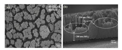 Figure 8 SEM image of top view (a) and cross-sectional view (b) of SiOx-TiO2 NRAs[68]
 Optical absorption measurement of deposited TiO2 NRAs and SiOx-TiO2 heterostructure samples was tested at room temperature. The wavelength range is 200-1100 nm. Fig. 9(a) is UV-vis absorption spectra of all samples. The enhancement in absorption has been found for SiOx-TiO2 compared to TiO2 over the whole region. Specifically, photon absorption value increased more than twice compared to pure TiO2 NRAs. And the suppression of transmission in Fig. 9(b) has also been measured in which heterostructure NRAs decreased a lot compared to TiO2 NRAs over the whole tested wavelength range[49, 69].
Figure 9
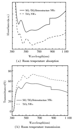 Figure 9 UV-Vis light spectra for all samples in absorption and transmission[68]
 4 Coupling with Noble MetalCoupling with noble metal has been regarded as one method to improve utilization efficiency of light resource. First, due to formation of Schottky barrier between metal and TiO2, the decoration could largely improve photoefficiency[70]. Hu et al.[71] have synthesised Pt-doped TiO2 which could improve greatly reaction activity with NOx oxidation. Ingram et al.[72] combined specific plasmon responded metal with semiconductor in order to hinder the recombination of electrons and holes. Some visible light responsed metal NPs like Ag and Au, could absorb UV-visible light strongly taking use of their plasmon resonance. Pu et al.[73] reported that some specific morphologies of Au decorated on TiO2 nanowire arrays largely enhanced the photocatalytic performance.
4.1 Ag NPs DecorationKumar et al.[74] have prepared the novel Ag NPs decorated TiO2 NRAs for photocatalyst and surface enhanced Raman scattering (SERS) applications. After the deposition of TiO2 NRs by GLAD techniques, Ag NPs were also deposited on top of the NRAs by the same physical method, as shown in Fig. 10[75].
Figure 10
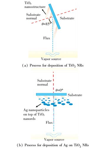 Figure 10 Process for deposition of TiO2 NRs deposition of Ag on TiO2 NRs[75]
 Fig. 11 shows Raman spectra with time goes by under light, and the intensity decreases gradually with lighter irradiation time. From the figure we can find that the intensity of Rh6G peak under UV irradiation prolonging until 90 min at 611 cm-1 decreases almost reaches to ~99%[76-77].
Figure 11
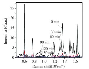 Figure 11 Raman spectra of Rh6G on Ag-TiO2 samples with longer irradiation time[75]
 4.2 Au/Pt CodecorationˇŞNoble Metallic NPs Deposition on TiO2 NRAsThe decoration of metallic NPs is still the previous one similar to CdS[58]. In Brief, we dipped the TiO2 NRAs substrates to HAuCl4 (or HPt2Cl6) and NaBH4 solutions successively[78]. Between two steps, the substrate was dipped in DI water to clean the residence which did not react. Here Au/Pt-TiO2 sample was decided to be decorated respectively 5 times.
Fig. 12 shows the TEM images of decorated NRAs and we can see that the size of Au and Pt NPs is ~4 nm. Herein lattice fringes of d=0.24 nm, 0.23 nm, 0.32 nm and 0.34 nm are corresponding to Au (111), Pt (111), rutile (110) and anatase (101). The junction between metal and semiconductor is thought to be helpful on interfacial charge transfer, and then improves photocatalytic activities of materials.
Figure 12
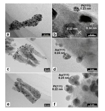 Figure 12 TEM images of (a-b) Pt decorated sample; (c-d) Au decorated sample and (e-f) Au/Pt co-decorated sample[78]
 The photodegradation of MO was used to test photocatalytic performance of samples. Here Fig. 13 shows the degradation of all samples. Au-TiO2 degraded ~20% MO after 120 illumination wike TiO2 and Pt-TiO2 do not show any activity. Because only Au could have plasmon reaction under visible lights. When combining Au and Pt NPs, the rate of MO photodegradation became to 1.36 times higher than single Au decorated sample. And from the results we can see that Pt NPs also improve the property on degradation. Au-Pt/TiO2 showed higher electrons and holes separation efficiency and present better performance.
Figure 13
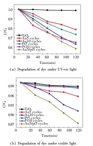 Figure 13 Degradation of dye under UV-vis light and visible light[78]
 5 Other Novel Methods5.1 Wrapped with TiO2 Atomic Layer Deposition (ALD)As we all know, charges excited by CdS QDs tend to be trapped which effected eventual results. In order to solve the problem, we put forward to coat a layer out of CdS QDs surface[79-80]. ALD is one method to deposit a quite thin layer of film which leads to reduce the surface recombination velocity and passivate the surface states[81]. Here, Xie et al.[82] design TiO2 NRAs/CdS QDs/ALD-TiO2 composite material coating an atomic layer out of TiO2 NRAs/CdS QDs to protect CdS.
During the ALD process, the substrate would be kept at 150 ˇć always. In brief, four dimethylamino titanium and water vapor were successively pumped into chamber several times to wait until reaction finished. And the precursor was controlled at specific temperature, respectively.
Here we change coated layers from 20 to 160. The TEM images are showed in Fig. 14. The CdS QDs have around 3 nm diameter and we can see the heterojunction between these two phases. HRTEM of TiO2 NRAs/CdS QDs/coated with 60c-ALD are presented in Figs. 14(c)-(d). And the layer wraps tightly around the substrate surface in which is about 2 nm thick. What's more, from TEM images coating with 80 ALD layers is thicker which reaches to 2.8 nm. The discoloration rates of MO are shown in Fig. 15. TiO2 NRAs/CdS QDs/coated with 60c-ALD-TiO2 owns the highest degradation rate of 7.47%, but the degradation rate is only 2.92% without coating. However, it can also be founded that, when coating more than 80, the degradation rate decreases badly. And mix of anatase and rutile also enhanced photocatalytic property[83].
Figure 14
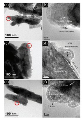 Figure 14 TEM images: (a, b) TiO2 NRAs/CdS QDs; and as-prepared sample (c, d) coated with 60 ALD TiO2; (e, f) coated with 60 ALD TiO2[82]
 Figure 15
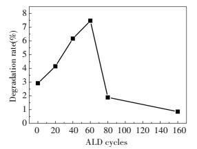 Figure 15 Visible light degradation result with different cycle number[82]
 5.2 Graphene Oxide-Ag/Ag2S-TiO2 Nanocomposites5.2.1 Ag/Ag2S NPs deposition on TiO2 NRAsOur recent work is about alternately coated Ag and Ag2S NPs on TiO2 NRAs respectively for specific times. Graphene oxide (GO) was prepared via modified Hummers method[84]. Ag/Ag2S-TiO2 NRs with substrates were immersed in this solution for few seconds. The samples were dried in a tube furnace at 50 ˇć to obtain the GO/Ag/Ag2S-TiO2 photocatalyst. GO-TiO2, GO/Ag-TiO2, GO/Ag2S-TiO2 were prepared in the similar way.
Furthermore, Fig. 16 showed TEM images of samples. From the bright dots we can see that Ag and Ag2S NPs were separately dispersed on the surface of TiO2. They are all in a regular elliptical shape. After the measurement of lattice fringes, d =0.233 nm, 0.244 nm, 0.345 nm and 0.325 nm match greatly to the interplanar spacing of Ag (111), Ag2S (200), anatase (101) and rutile (110), respectively. The heterojunctions of metal and oxide, including Ag-TiO2, could be helpful to interfacial charge transfer. Furthermore, anatase-rutile heterojunction also enhances the improvement of photon-induced electrons and hinders the charge recombination[85].
Figure 16
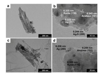 Figure 16 TEM images of (a-b) Ag/Ag2S-TiO2 NRAs; (c-d) GO/Ag/Ag2S-TiO2 NRAs
 5.2.2 Photodegradation of MOTo evaluate the effect of composite decoration, MO degradation was also tested. For comparison, we also tested Ag/Ag2S-TiO2 NRAs, Ag-TiO2 NRAs, Ag2S-TiO2 NRAs and TiO2 NRAs. What's more, all these samples just combined with GO were also tested. From Table 1, TiO2 NRAs and GO-TiO2 NRAs did not degrade dye moleculars obviously due to nonaborbance of TiO2 in visible light, while 8.17%, 7.15% and 14.83% of MO were degraded by Ag-TiO2 NRAs, Ag2S-TiO2 and Ag/Ag2S-TiO2 NRAs after 120 min illumination under visible lights. These results indicated that both Ag and Ag2S NPs can be active under visible light. The higher activity of Ag/Ag2S-TiO2 can be attributed to the photoexcited Ag2S semiconductor and plasmon-induced Ag NPs. Moreover, further enhancement of photocatalytic activities can be observed after the introduction of GO. No matter what kind of combinations, after covered by GO, those photocatalytic degradation efficiencies are improved by 200%-300%. With the combination of GO/Ag/Ag2S-TiO2 NRAs, the degradation efficiency of MO increased and reached maximum to 41.79%. Therefore, GO enhanced greatly on photocatalytic property.
±í 1
TiO20
GO-TiO20
Ag-TiO28.17
GO/Ag-TiO221.88
Ag2S-TiO27.15
GO/Ag2S-TiO218.74
Ag/Ag2S-TiO214.83
GO/Ag/Ag2S-TiO241.79
Table 1 Degradation efficiency of MO under 120 min-visible light irradiation
5.2.3 Photocatalytic mechanismBased on the above results and measurement, the photocatalytic mechanism of Ag/Ag2S/GO-TiO2 NRs was proposed. In the composite, Ag and Ag2S NPs are active to visible light. The higher activity of GO/Ag/Ag2S-TiO2 NRs is contributed by the photoexcited Ag2S semiconductor, plasmon-induced Ag NPs, and effective electron-hole separation of GO. Under visible light irradiation, the incident photons are absorbed by Ag NPs. Then, electrons produced move to the CB of TiO2. Meanwhile, Ag2S NPs are excited to form electrons and holes. Considering the CB of Ag2S is more positive than that of TiO2[86-87], electrons generated from Ag2S also tend to transfer into the CB of TiO2. In the presence of GO, due to perfect sp2-hybridized two-dimensional carbon structure and larger surface area[9, 88], electrons in the CB of TiO2 can further quickly transfer by GO as well as Ag NPs. In turn it would reduce the recombination of photo-generated electrons and holes. Then electrons can either reduce the dye or can react with electron acceptors. The reaction process is presented in Fig. 17.
Figure 17
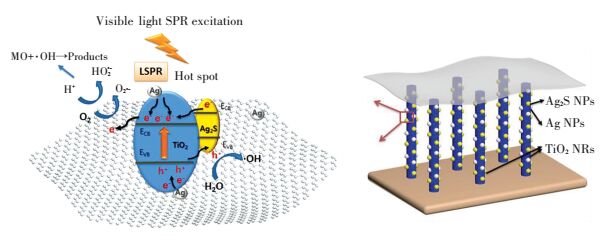 Figure 17 The schematic of degradation for GO/Ag/Ag2S-TiO2 NRAs on MO
 6 ConclusionsMost photocatalysts are usually powders in past reports, which are hard to collect after reaction. Here we report GLAD method of NRs on specific substrates to form self-standing structures, which makes catalysts easier to recycle. Furthermore, it also holds back secondary pollution and improves the efficiency of recycles. In this review, we have introduced four main method of introducing dopants, decorating band gap matched materials, combining with noble metals, and covering with GO or ALD layer to make TiO2 be more efficient under visible irradiation. Such researches illustrate we can obtain better performance according to rational design of composite nanostructures. And our survey also demonstrates that GLAD methods have huge potential on fabricating photocatalysts and accomplishing better utilization of solar irradiation.
References
[1] Kuang P Y, Zheng P Y, Liu Z Q, et al. Embedding Au quantum dots in rimous cadmium sulfide nanospheres for enhanced photocatalytic hydrogen evolution. Small, 2016, 12(48): 6735-6744. DOI:10.1002/smll.201602870 (
 0)
0)[2] Akhter P, Farkhondehfal M A, Hernandez S, et al. Environmental issues regarding CO2 and recent strategies for alternative fuels through photocatalytic reduction with titania-based materials. Journal of Environmental Chemical Engineering, 2016, 4(4): 3934-3953. DOI:10.1016/j.jece.2016.09.004 (
 0)
0)[3] Cui D H, Huang W Z, Li Y Y, et al. Hydrothermal preparation and photocatalytic activity of Zn1-xCdxS solid solution nanoparticles. Current Nanoscience, 2015, 12(4): 508-513. DOI:10.2174/1573413712666151210230551 (
 0)
0)[4] Chen S, Zhang F. Recent progress on photocatalysts with wide visible light range absorption for heterogeneous water splitting. Chinese Journal of Catalysis, 2014, 35(9): 1431-1432. DOI:10.1016/s1872-2067(14)60183-2 (
 0)
0)[5] Wu J, Huang F, L¨ą X, et al. One-pot synthesis of BiSbO4 nanophotocatalyst with enhanced visible-light performance. Crystengcomm, 2011, 13: 3920-3924. DOI:10.1039/c1ce05025g (
 0)
0)[6] Low J, Cheng B, Yu J. Surface modification and enhanced photocatalytic CO2 reduction performance of TiO2: a review. Applied Surface Science, 2017, 392: 658-686. DOI:10.1016/j.apsusc.2016.09.093 (
 0)
0)[7] Gholipour M R, Beland F, Do T O. Post-calcined carbon nitride nanosheets as an efficient photocatalyst for hydrogen production under visible light irradiation. ACS Sustainable Chemistry & Engineering, 2017, 5(1): 213-220. DOI:10.1021/acssuschemeng.6b01282 (
 0)
0)[8] Riley M J, Williams B, Condon G Y, et al. Photocatalytic properties of porous titania grown by oblique angle deposition. Journal of Applied Physics, 2012, 111(7): 8269-8285. DOI:10.1063/1.3699370 (
 0)
0)[9] Zhou Q, Li Z C, Ni J, et al. A simple model to describe the rule of glancing angle deposition. Materials Transactions, 2011, 52(3): 469-473. DOI:10.2320/matertrans.m2010342 (
 0)
0)[10] Li Z C, Zhu Y, Zhou Q, et al. Photocatalytic properties of TiO2 thin films obtained by glancing angle deposition. Applied Surface Science, 2012, 258(7): 2766-2770. DOI:10.1016/j.apsusc.2011.10.129 (
 0)
0)[11] Horprathum M. Fabrication of nanostructure by physical vapor deposition with glancing angle deposition technique and its applications. American Institute of Physics Conference Proceedings. Melville, NY: AIP Publishing, 2008, 167(8): 7-11. DOI: 10.1063/1.4897091. (
 0)
0)[12] Mukherjee S, Gall D. Structure zone model for extreme shadowing conditions. Thin Solid Films, 2013, 527: 158-163. DOI:10.1016/j.tsf.2012.11.007 (
 0)
0)[13] Hall J Z, Taschuk M T, Brett M J. Polarity-adjustable reversed phase ultrathin-layer chromatography. Journal of Chromatography A, 2012, 1266: 168-174. DOI:10.1016/j.chroma.2012.10.020 (
 0)
0)[14] Hung K H, Chiou G D, Wong M S, et al. Transparent sculptured titania films for enhanced light absorption in thin-film Si solar cells. Thin Solid Films, 2011, 520(5): 1385-1389. DOI:10.1016/j.tsf.2011.10.038 (
 0)
0)[15] Basnet P, Zhao Y P. Tuning the CuxO nanorod composition for efficient visible light induced photocatalysis. Catalysis Science & Technology, 2016, 6: 2228-2238. DOI:10.1039/c5cy01464f (
 0)
0)[16] Basnet P, Larsen G K, Jadeja R P, et al. alpha-Fe2O3 nanocolumns and nanorods fabricated by electron beam evaporation for visible light photocatalytic and antimicrobial applications. ACS Applied Materials Interfaces, 2013, 5(6): 2085-2095. DOI:10.1021/am303017c (
 0)
0)[17] Ferreira A, Borges J, Nartin L N, et al. Piezoresistive response of nano-architectured TixCuy thin films for sensor applications. Sensors and Actuators A: Physical, 2016, 247: 105-114. DOI:10.1016/j.sna.2016.05.033 (
 0)
0)[18] Rahchamani S Z, Dizaji H R, Ehsani M H. Study of structural and optical properties of ZnS zigzag nanostructured thin films. Applied Surface Science, 2015, 356: 1096-1104. DOI:10.1016/j.apsusc.2015.08.224 (
 0)
0)[19] Rahchamani S Z, Dizaji H R G, Ehsani M H. Fabrication of ZnS zigzag sculptured nanostructured thin films. Procedia Materials Science, 2015, 11: 464-468. DOI:10.1016/j.mspro.2015.11.055 (
 0)
0)[20] Pedrosa P, Machado D, Fiedler P, et al. Electrochemical characterization of nanostructured Ag:TiN thin films produced by glancing angle deposition on polyurethane substrates for bio-electrode applications. Journal of Electroanalytical Chemistry, 2016, 768: 110-120. DOI:10.1016/j.jelechem.2016.03.005 (
 0)
0)[21] Sorge J B, Taschuk M T, Wakefield N G, et al. Metal oxide morphology in argon-assisted glancing angle deposition. Journal of Vacuum Science & Technology A:Vacuum Surfaces & Films, 2012, 30(2): 021507. DOI:10.1116/1.3687204 (
 0)
0)[22] Krause K M, Taschuk M T, Brett M J. Glancing angle deposition on a roll: Towards high-throughput nanostructured thin films. Journal of Vacuum Science & Technology A: Vacuum, Surfaces, and Films, 2013, 31(3): 031507. DOI:10.1116/1.4798947 (
 0)
0)[23] Yildiz A, Cansizoglu H, Turkoz M, et al. Glancing angle deposited Al-doped ZnO nanostructures with different structural and optical properties. Thin Solid Films, 2015, 589: 764-769. DOI:10.1016/j.tsf.2015.06.058 (
 0)
0)[24] Wakefield N, Sit J. Three-dimensional alignment of liquid crystals in nanostructured porous thin films. Proc. SPIE 6654, Liquid Crystals XI. Bellingham WA : SPIE, 2007, 6654: 665404. DOI: 10.1117/12.735265. (
 0)
0)[25] Van Dijken J G, Wu N L-W, Fleischauer M D, et al. Morphology control and nanoscale patterning of small molecule organic thin films. Proc. SPIE 8435, Organic Photonics V, 84350R. Bellingham WA : SPIE, 2012. 84350R. DOI: 10.1117/12.922659. (
 0)
0)[26] Gerein N J. Nanostructured titanium dioxide/polytiophene photovoltaic devices. Proceedings of the Photovoltaic Specialists Conference, 2008. PVSC ˇä08. 33rd IEEE. Piscataway: IEEE, 2008. 1-6. DOI: 10.1109/pvsc.2008.4922626. (
 0)
0)[27] Gish D A, Summers M A, Jensen M O, et al. Enhanced Control of Morphology in Thin Film Nanostructure Arrays. Proceedings of the 2006 IEEE Conference on Emerging Technologies-Nanoelectronics. Piscataway: IEEE, 2006. 447-451. DOI: 10.1109/nanoel.2006.1609768. (
 0)
0)[28] Xu S, Wang C, Francis S A, et al. Glancing angle deposited Ni nanopillars coated with conformal, thin layers of Pt by a novel electrodeposition: Application to the oxygen reduction reaction. Electrochim Acta, 2015, 151: 537-543. DOI:10.1016/j.electacta.2014.11.028 (
 0)
0)[29] Yuan F, Li Z, Zhang T, et al. Enhanced light absorption of amorphous silicon thin film by substrate control and ion irradiation. Nanoscale Research Letters, 2014, 9: 173. DOI:10.1186/1556-276x-9-173 (
 0)
0)[30] Lalany A, Tucker R T, Taschuk M T. Axial resistivity measurement of a nanopillar ensemble using a cross-bridge Kelvin architecture. Journal of Vacuum Science & Technology A: Vacuum, Surfaces, and Films, 2013, 31(3): 031502. DOI:10.1116/1.4794182 (
 0)
0)[31] Jen Y J, Liao H S, Lin M J. Size effect of aluminum / silicon-dioxide / aluminum nanosandwich films for negative optical properties. Proceedings of the SPIE 8818, Nanostructured Thin Films ˘ö. Bellingham WA : SPIE, 2013. 881817. DOI: 10.1117/12.2023993. (
 0)
0)[32] Rider D A, Tucker R T, Worfolk B J, et al. Indium tin oxide nanopillar electrodes in polymer/fullerene solar cells. Nanotechnology, 2011, 22(8): 085706. DOI:10.1088/0957-4484/22/8/085706 (
 0)
0)[33] Fujishima A, Honda K. Electrochemical photolysis of water at a semiconductor electrode. Nature, 1972, 238(5358): 37-38. DOI:10.1038/238037a0 (
 0)
0)[34] Yuan R, Chen T, Fei E, et al. Surface Chlorination of TiO2-based photocatalysts: A way to remarkably improve photocatalytic activity in both UV and visible region. ACS Catalysis, 2011, 1(3): 200-206. DOI:10.1021/cs100122v (
 0)
0)[35] Pihosh Y, Trukevych I, Ye J, et al. Physical and photocatalytic properties of TiO2 nanostructures fabricated by means of glancing angle deposition. ECS Transactions, 2009, 16(25): 49-58. DOI:10.1149/1.3115522 (
 0)
0)[36] Barborini E, Conti A M, Kholmanov I, et al. Nanostructured TiO2 films with 2 eV optical gaps. Advanced Materials, 2005, 17(15): 1842-1846. DOI:10.1002/adma.200401169 (
 0)
0)[37] Zhang J Y, Zhu H L, Zheng S K, et al. TiO2 film/Cu2O microgrid heterojunction with photocatalytic activity under solar light irradiation. ACS Applied & Materials Interfaces, 2009, 1(10): 2111-2114. DOI:10.1021/am900463g (
 0)
0)[38] Higashimoto S, Sakiyama M, Azuma M. Photoelectrochemical properties of hybrid WO3/TiO2 electrode. Effect of structures of WO3 on charge separation behavior. Thin Solid Films, 2006, 503(1/2): 201-206. DOI: 10.1016/j.tsf.2005.11.110. (
 0)
0)[39] Tian Y, Tatsuma T. Mechanisms and applications of plasmon-induced charge separation at TiO2 films loaded with gold nanoparticles. Journal of the American Chemical Society, 2005, 127(20): 7632-7637. DOI:10.1021/ja042192u (
 0)
0)[40] Low C T J, de Leon C P, Walsh F C. The reduction of hydrogen peroxide at an Au-coated nanotubular TiO2 array. Journal of Applied Electrochemistry, 2014, 44(1): 169-177. DOI:10.1007/s10800-013-0623-5 (
 0)
0)[41] Hirakawa T, Kamat P V. Photoinduced electron storage and surface plasmon modulation in Ag@TiO2 clusters. Langmuir, 2004, 20(14): 5645-5647. DOI:10.1021/la048874c (
 0)
0)[42] Akhavan O. Lasting antibacterial activities of Ag-TiO2/Ag/a-TiO2 nanocomposite thin film photocatalysts under solar light irradiation. Journal of Colloid and Interface Science, 2009, 336(1): 117-124. DOI:10.1016/j.jcis.2009.03.018 (
 0)
0)[43] Ihara T. Preparation of a visible-light-active TiO2 photocatalyst by RF plasma treatment. Journal of Materials Science, 2001, 36(17): 4201-4207. DOI:10.1023/A:1017929207882 (
 0)
0)[44] Umebayashi T, Yamaki T, Itoh H, et al. Band gap narrowing of titanium dioxide by sulfur doping. Applied Physics Letters, 2002, 81(3): 454-456. DOI:10.1063/1.1493647 (
 0)
0)[45] Miyauchi M, Ikezawa A, Tobimatsu H, et al. Zeta potential and photocatalytic activity of nitrogen doped TiO2 thin films. Physical Chemistry Chemical Physics, 2004, 6: 865-870. DOI:10.1039/b314692h (
 0)
0)[46] Shieh D L, Lin Y S, Yeh J H, et al. N-doped, porous TiO2 with rutile phase and visible light sensitive photocatalytic activity. Chemical Communications, 2012, 48: 2528-2530. DOI:10.1039/c2cc16960f (
 0)
0)[47] Ohno T, Akiyoshi M, Umebayashi T, et al. Preparation of S-doped TiO2 photocatalysts and their photocatalytic activities under visible light. Applied Catalysis A: General, 2004, 265(1): 115-121. DOI:10.1016/j.apcata.2004.01.007 (
 0)
0)[48] Ho W, Yu J C, Lee S. Synthesis of hierarchical nanoporous F-doped TiO2 spheres with visible light photocatalytic activity. Chemical Communications, 2006(10): 1115-1117. DOI:10.1039/b515513d (
 0)
0)[49] Asahi R, Morikawa T, Ohwaki T, et al. Visible-light photocatalysis in nitrogen-doped titanium oxides. Science, 2001, 293(5528): 269-271. DOI:10.1126/science.1061051 (
 0)
0)[50] Xie Z, Zhang Y, Liu X, et al. Visible light photoelectrochemical properties of N-doped TiO2 nanorod arrays from TiN. Journal of Nanomaterials, 2013(2013): Article ID 930950. DOI: 10.1155/2013/930950. (
 0)
0)[51] Miyata N, Akiyoshi S. Preparation and electrochromic properties of Rf-Sputtered molybdenum Oxide-Films. Journal of Applied Physics, 1985, 58(4): 1651-1655. DOI:10.1063/1.336307 (
 0)
0)[52] Tucker R T, Beckers N A, Fleischauer M D, et al. Electron beam deposited Nb-doped TiO2 toward nanostructured transparent conductive thin films. Thin Solid Films, 2012, 525: 28-34. DOI:10.1016/j.tsf.2012.10.075 (
 0)
0)[53] Xiao X D, Miao L, Xu G, et al. Microstructure and optical properties of Sm3+ doped TiO2 thin films by oblique angle deposition. Integrated Ferroelectrics, 2011, 129(1): 201-207. DOI:10.1080/10584587.2011.576950 (
 0)
0)[54] Lee H J, Chen P, Moon S J, et al. Regenerative PbS and CdS quantum dot sensitized solar cells with a cobalt complex as Hole mediator. Langmuir, 2009, 25(13): 7602-7608. DOI:10.1021/la900247r (
 0)
0)[55] Cheng S. Photoelectrochemical performance of multiple semiconductors (CdS/CdSe/ZnS) cosensitized TiO2 photoelectrodes. Journal of Physical Chemistry C, 2012, 116(3): 2615-2621. DOI:10.1021/jp209258r (
 0)
0)[56] Guijarro N, Campina J M, Shen Q, et al. Uncovering the role of the ZnS treatment in the performance of quantum dot sensitized solar cells. Physical Chemistry Chemical Physics, 2011, 13: 12024-12032. DOI:10.1039/C1CP20290A (
 0)
0)[57] Li G S, Zhang D Q, Yu J C. A new visible-light photocatalyst: CdS quantum dots embedded mesoporous TiO2. Environmental Science Technology, 2009, 43(18): 7079-7085. DOI:10.1021/es9011993 (
 0)
0)[58] Baker D R, Kamat P V. Photosensitization of TiO2 nanostructures with CdS quantum dots: Particulate versus tubular support architectures. Advance Functional Materials, 2009, 19: 805-811. DOI:10.1002/adfm.200801173 (
 0)
0)[59] Das K, De S K. Optical properties of the type-˘ň core-ell TiO2@CdS nanorods for photovoltaic applications. Journal of Physical Chemistry C, 2011, 113(9): 3494-3501. DOI:10.1021/jp8083953 (
 0)
0)[60] Liu Y, Zhou H, Zhou B, et al. Highly stable CdS-modified short TiO2 nanotube array electrode for efficient visible-light hydrogen generation. International Journal of Hydrogen Energy, 2011, 36(1): 167-174. DOI:10.1016/j.ijhydene.2010.09.089 (
 0)
0)[61] Zhou H L, Qu Y Q, Zeid T, et al. Towards highly efficient photocatalysts using semiconductor nanoarchitectures. Energgy & Environmental Science, 2012, 5: 6732-6743. DOI:10.1039/c2ee03447f (
 0)
0)[62] Xie Z, Liu X, Wang W, et al. Enhanced photoelectrochemical and photocatalytic performance of TiO2 nanorod arrays/CdS quantum dots by coating TiO2 through atomic layer deposition. Nano Energy, 2015, 11: 400-408. DOI:10.1016/j.nanoen.2014.11.024 (
 0)
0)[63] Salvador P. Hole diffusion length inn-TiO2 single crystals and sintered electrodes: Photoelectrochemical determination and comparative analysis. Journal of Applied Physics, 1984, 55(8): 2977-2985. DOI:10.1063/1.333358 (
 0)
0)[64] Cheng P, Deng C, Gu M, et al. Visible-light responsive zinc ferrite doped titania photocatalyst for methyl orange degradation. Journal of Materials Science, 2007, 42(22): 9239-9244. DOI:10.1007/s10853-007-1902-5 (
 0)
0)[65] Jin S F, Li Y Z, Xie H, et al. Highly selective photocatalytic and sensing properties of 2D-ordered dome films of nano titania and nano Ag2+ doped titania. Journal of Materials Chemistry, 2012, 22(4): 1469-1476. DOI:10.1039/c1jm14216j (
 0)
0)[66] Xie Y, Ali G, Yoo S H, et al. Sonication-assisted synthesis of CdS quantum-dot-sensitized TiO2 nanotube arrays with enhanced photoelectrochemical and photocatalytic activity. ACS Applied Materials & Interfaces, 2010, 2(10): 2910-2914. DOI:10.1021/am100605a (
 0)
0)[67] Li Z C, Xiong S, Wang G, et al. Role of Ag2S coupling on enhancing the visible-light-induced catalytic property of TiO2 nanorod arrays. Scientific Reports-Uk, 2016, 6: 19754. DOI:10.1038/srep19754 (
 0)
0)[68] Dhar J C, Mondal A, Singh N K, et al. Enhanced photoemission from glancing angle deposited SiOx-TiO2 axial heterostructure nanowire arrays. Journal of Applied Physics, 2013, 113(17): 174304. DOI:10.1063/1.4803550 (
 0)
0)[69] Khan S U M, Al-Shahry M, Jr Ingler W B. Efficient photochemical water splitting by a chemically modified n-TiO2. Science, 2002, 297(5590): 2243-2245. DOI:10.1126/science.1075035 (
 0)
0)[70] Meng Z D, Zhu L, Choi J G, et al. Effect of Pt treated fullerene/TiO2 on the photocatalytic degradation of MO under visible light. J Mater Chem, 2011, 21: 7596-7603. DOI:10.1039/C1JM10301F (
 0)
0)[71] Hu Y, Song X, Jiang S M, et al. Enhanced photocatalytic activity of Pt-doped TiO2 for NOx oxidation both under UV and visible light irradiation: A synergistic effect of lattice Pt4+ and surface PtO. Chemical Engineering Journal, 2015, 274: 102-112. DOI:10.1016/j.cej.2015.03.135 (
 0)
0)[72] Ingram D B, Linic S. Water splitting on composite plasmonic-metal/semiconductor photoelectrodes: evidence for selective plasmon-induced formation of charge carriers near the semiconductor surface. Journal of the American Chemical Society, 2011, 133(14): 5202-5205. DOI:10.1021/ja200086g (
 0)
0)[73] Pu Y C, Wang G, Chang K D, et al. Au nanostructure-decorated TiO2 nanowires exhibiting photoactivity across entire UV-visible region for photoelectrochemical water splitting. Nano Letters, 2013, 13(8): 3817-3823. DOI:10.1021/nl4018385 (
 0)
0)[74] Kumar S, Lodhi D K, Singh J P. Highly sensitive multifunctional recyclable Ag-TiO2 nanorod SERS substrates for photocatalytic degradation and detection of dye molecules. RSC Advances, 2016, 6: 45120-45126. DOI:10.1039/c6ra06163j (
 0)
0)[75] Xu J X, Xiao X, Ren F, et al. Enhanced photocatalysis by coupling of anatase TiO2 film to triangular Ag nanoparticle island. Nanoscale Research Letters, 2012, 7: 239. DOI:10.1186/1556-276x-7-239 (
 0)
0)[76] Han X X, Jia H Y, Wang Y F, et al. Analytical technique for label-free multi-protein detection-based on Western blot and surface-enhanced Raman scattering. Analytical Chemistry, 2008, 80(8): 2799-2804. DOI:10.1021/ac702390u (
 0)
0)[77] Zhao X, Zhang B, Ai K, et al. Monitoring catalytic degradation of dye molecules on silver-coated ZnO nanowire arrays by surface-enhanced Raman spectroscopy. Journal of Materials Chemistry, 2009, 19: 5547-5553. DOI:10.1039/b902883h (
 0)
0)[78] Shuang S, Lv R, Xie Z, et al. Surface plasmon enhanced photocatalysis of Au/Pt-decorated TiO2 nanopillar arrays. Scientific Reports-Uk, 2016, 6: Article No 26670. DOI: 10.1038/srep26670. (
 0)
0)[79] Tang W Z, Huang C P. Photocatalyzed oxidation pathways of 2, 4-dichlorophenol by CdS in basic and acidic aqueous-solutions. Water Research, 1995, 29(2): 745-756. DOI:10.1016/0043-1354(94)00151-v (
 0)
0)[80] Yu K, Lin X, Lu G, et al. Optimized CdS quantum dot-sensitized solar cell performance through atomic layer deposition of ultrathin TiO2 coating. RSC Advances, 2012, 2: 7843-7848. DOI:10.1039/c2ra20979a (
 0)
0)[81] Roelofs K E, Brennan T P, Dominguez J C, et al. Effect of Al2O3 recombination barrier layers deposited by atomic layer deposition in solid-state CdS quantum dot-sensitized solar cells. Journal of Physical Chemistry C, 2013, 117(11): 5584-5592. DOI:10.1021/jp311846r (
 0)
0)[82] Xie Z, Liu X, Wang W, et al. Enhanced photoelectrochemical and photocatalytic performance of TiO2 nanorod arrays/CdS quantum dots by coating TiO2 through atomic layer deposition. Nano Energy, 2015, 11: 400-408. DOI:10.1016/j.nanoen.2014.11.024 (
 0)
0)[83] Kang Q, Cao J, Zhang Y, et al. Reduced TiO2 nanotube arrays for photoelectrochemical water splitting. Journal of Materials Chemistry A, 2013, 1: 5766-5774. DOI:10.1039/C3TA10689F (
 0)
0)[84] Cui X, Yang S, Yan X, et al. Pyridinic-Nitrogen-Dominated Graphene Aerogels with Fe-N-C Coordination for Highly Efficient Oxygen Reduction Reaction. Advanced Functional Materials, 2016, 26(31): 5708-5717. DOI:10.1002/adfm.201601492 (
 0)
0)[85] Wang Y, Shi R, Lin J, et al. Significant photocatalytic enhancement in methylene blue degradation of TiO2 photocatalysts via graphene-like carbon in situ hybridization. Applied Catalysis B: Environmental, 2010, 100(1/2): 179-183. DOI:10.1016/j.apcatb.2010.07.028 (
 0)
0)[86] Pant H R, Pant B, Kim H J, et al. A green and facile one-pot synthesis of Ag ZnO/RGO nanocomposite with effective photocatalytic activity for removal of organic pollutants. Ceramics International, 2013, 39(5): 5083-5091. DOI:10.1016/j.ceramint.2012.12.003 (
 0)
0)[87] Pal S, Tak Y K, Song J M, et al. Does the antibacterial activity of silver nanoparticles depend on the shape of the nanoparticle? A study of the Gram-negative bacterium Escherichia coli. Applied and Environmental Microbiology, 2007, 73(6): 1712-1720. DOI:10.1128/AEM.02218-06 (
 0)
0)[88] Liu J, Bai H, Wang Y, et al. Self-Assembling TiO2 Nanorods on large graphene oxide sheets at a two-phase interface and their anti-recombination in photocatalytic applications. Advanced Functional Materials, 2010, 20(23): 4175-4181. DOI:10.1002/adfm.201001391 (
 0)
0)